Part Number: TIDA-00951
Hi,
I have couple of questions on the boost mode,
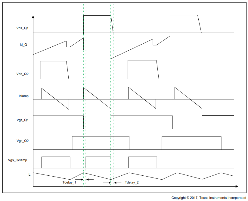
- What is the purpose of delay_1 and Tdelay_2 ?
- there is need to be ZVS is the transistors on the low side?
A very large power losses are created on the transistors during the "power boost" of 500W.
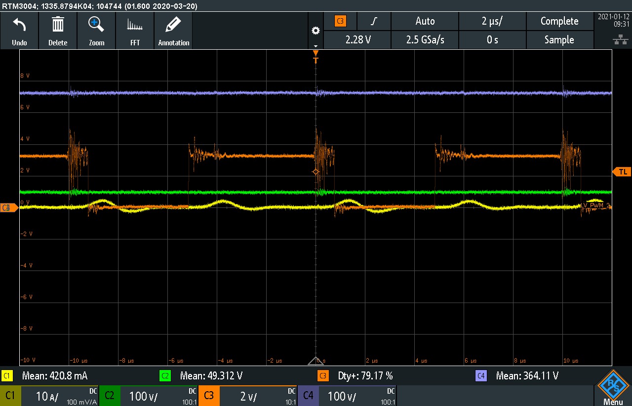
Another issue that i am facing is that i can see a lot of noise on the tida 00281 LV1 and LV2 leg, therefore the signal at the output of the DSP, I an suspect that there is an issue with the buffer between the DSP and the transistor. can you please assert me if this noise is normal (Orange signal)?
Thank you and Best Regards,
Michael