This thread has been locked.

If you have a related question, please click the "Ask a related question" button in the top right corner. The newly created question will be automatically linked to this question.

TIDA-010056: Without Connecting Hall Sensor run the code

Part Number: TIDA-010056
Other Parts Discussed in Thread: MSP430FR2355, DRV8350R, DRV8323, DRV8350, DRV8353

Hello TI Helpers,

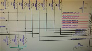
I am using TIDA-010056. In which I have not connected BLDC motor to the hardware. I have also not connected Hall Sensors of BLDC motor to TIDA-010056. Just I want to check only waveforms on MOSFET side in free running mode ( without connecting BLDC motor and Hall Sensors ). 

So what things I have to change in CCS programe code (given by TI for TIDA-010056) ?  

If you give updated program ( without connecting hall sensors and BLDC) it will be great help.

Thank you in advance.

  • Hi Sudhir,

    An easy way to do this is by providing the hall sensor signals, HA, HB, HC to logic voltage levels externally. You don't need a hall sensor, but connect the pins HA, HB, HC to known signal levels. A logic high is 3.3V and logic low is GND. The states HA=HB=HC=3.3V  (logic high), and HA=HB=HC=0V (logic low) are invalid states. Any other state will enable corresponding MOSFETs to turn on and off as per the BLDC trap control sequence. The on board 3.3V can be used.

    The code has blocked rotor protection and that needs to be disabled. One way to do this is by commenting the statement  " Block_Rotor_Counter++;" in the TIMER B interrupt subroutine. If you are familiar with the code, you can disable blocked rotor protection in other ways.

    I would recommend to learn the code to proceed on testing.

    Regards,

    Manu

  • I'm looking for compact hall-effect sensors, similar to what is found on the VKB and Virpil bases that measure shaft rotation. These are board mounted sensors, and I'm looking for something similar, already mounted to a small PCB such that I can simply run wires to it without having to precisely solder a small chip and make a custom PCB.

    Does anyone have experience working with these? I'm not an electronics guru (I prefer mechanical design) so I'm sure there's going to have to be some handholding.

  • Hii Manu Balakrishnan,

    Thank you for your quick response.

    Can you please share the code lines which we have to modify in TIDA-010056 code.

    We have attached the code. If you modify the code it will be great help.

    Thank you in advance.


    /* --COPYRIGHT--,
    * Copyright (c) 2019, Texas Instruments Incorporated
    * All rights reserved.
    *Modified by : A0132403
    *Modified Date: 30th April 2019
    *Modified * Redistribution and use in source and binary forms, with or without
    * modification, are permitted provided that the following conditions
    * are met:
    *
    * * Redistributions of source code must retain the above copyright
    * notice, this list of conditions and the following disclaimer.
    *
    * * Redistributions in binary form must reproduce the above copyright
    * notice, this list of conditions and the following disclaimer in the
    * documentation and/or other materials provided with the distribution.
    *
    * * Neither the name of Texas Instruments Incorporated nor the names of
    * its contributors may be used to endorse or promote products derived
    * from this software without specific prior written permission.

    * THIS SOFTWARE IS PROVIDED BY THE COPYRIGHT HOLDERS AND CONTRIBUTORS "AS IS"
    * AND ANY EXPRESS OR IMPLIED WARRANTIES, INCLUDING, BUT NOT LIMITED TO,
    * THE IMPLIED WARRANTIES OF MERCHANTABILITY AND FITNESS FOR A PARTICULAR
    * PURPOSE ARE DISCLAIMED. IN NO EVENT SHALL THE COPYRIGHT OWNER OR
    * CONTRIBUTORS BE LIABLE FOR ANY DIRECT, INDIRECT, INCIDENTAL, SPECIAL,
    * EXEMPLARY, OR CONSEQUENTIAL DAMAGES (INCLUDING, BUT NOT LIMITED TO,
    * PROCUREMENT OF SUBSTITUTE GOODS OR SERVICES; LOSS OF USE, DATA, OR PROFITS;
    * OR BUSINESS INTERRUPTION) HOWEVER CAUSED AND ON ANY THEORY OF LIABILITY,
    * WHETHER IN CONTRACT, STRICT LIABILITY, OR TORT (INCLUDING NEGLIGENCE OR
    * OTHERWISE) ARISING IN ANY WAY OUT OF THE USE OF THIS SOFTWARE,
    * EVEN IF ADVISED OF THE POSSIBILITY OF SUCH DAMAGE.
    *
    ***********************************************************************************
    // System Configuration
    // Device Part Number : MSP430FR2355
    // compiler : Code Composer Studio v8.3.0
    // Oscillator Frequency : 24MHz, using internal DCO
    // PWM generation : TIMER: TB3.1 –TB.6, Clock = 25 MHz, PWM frequency set for 20kHz
    20 kHz
    //
    // Position Feedback : Hall sensors signals
    // HA -> P3.0
    // HB -> P3.1
    // HC -> P3.2
    *
    // ADC : A0 -> Speed reference from the external potentiometer/trigger
    // A6 -> Phase A back EMF sensing for sensorless
    // A5 -> Phase B back EMF sensing for sensorless
    // A4 -> Phase C back EMF sensing for sensorless
    // A7 -> DC bus voltage sensing
    // A8 -> Low-side DC bus current sensing
    // A9 -> PCB or FET temperature feedback
    *
    *
    //Comparator configuration for back EMF zero crossing detection : CB2/P1.2 -> IDC
    // COMP0.O (P2.0) – Phase A back EMF zero cross comparator
    // COMP1.O(P2.1) – Phase C back EMF zero cross comparator
    // OA1O (P1.5) - Phase C back EMF zero cross comparator. The
    //opamp of smart compo module is configured as a comparator
    *
    //DRV8350RS - SPI programming pins connection
    // P4.4 -> SCS
    // P4.5 -> SCLK
    // P4.6 -> SDO
    // P4.7 -> SDI
    *
    //UART communication
    // P4.2 -> UART RX pin
    // P4.3 -> UART TX pin
    //MCU Digital Inputs/Output
    // P5.4 -> Direction of motor rotation
    // P4.1 -> ENABLE connection for DRV8350R
    // P4.0 -> FAULT pin connection from DRV8350R
    // P2.6 -> LED output

    ***********************************************************************************/

    //Header Files//
    #include "msp430fr2355.h"
    #include "stdint.h"

    #define CALTDH0CTL1_256 *((unsigned int *)0x1A36)

    /*****************************InstaSPIN**************************************/


    #define PWM_PERIOD 600 //PWM Frequency (Hz) = 25MHz/((2*PWM_PERIOD)-1)
    #define MAX_DUTYCYCLE 600 //relative to PWM_PERIOD
    #define MIN_DUTYCYCLE 5 //relative to PWM_PERIOD
    #define ACCEL_RATE 100 //Ramp up time to full scale duty cycle = (Full scale duty cycle) * ACCEL_RATE * PWM_PERIOD/PWM_Frequency
    #define DEAD_TIME_MCU 1 // Dead time from MSP430 = DEAD_TIME* 0.0625 uS (for 16MHz clock)
    #define Block_Rotor_Duration 800 //Blocked_rotor shut off time (s) = Block_Rotor_Duration*30000/Timer clock frequency

    /*************************************program variables**********************************************/
    unsigned int DC_BUS_CURRENT = 0;
    unsigned int DC_Bus_Voltage = 0;
    unsigned int SPEED_REF = 0;
    unsigned int Temperature_feedback = 0;
    unsigned int start_count = 0;
    unsigned int HALL_STATE = 0;
    unsigned int softstart_counter = 0;
    unsigned int CurrentDutyCycle = 100;
    unsigned int DIRECTION = 0 ;
    unsigned int FirstADC_flag = 1;
    unsigned int ADC_selection_flag = 1;
    unsigned int ADC_selection_flag_1 = 1;
    unsigned int Block_Rotor_Counter = 0;
    unsigned int Block_Rotor_Counter_1 =0;
    unsigned int ADC_RESULT = 0;

    unsigned int commutation_time = 0;
    unsigned int commutation_time_counter = 0;
    unsigned int advance_angle_time_counter = 0;
    unsigned int advance_angle_time = 0;
    unsigned int commutation_done = 0;
    unsigned int Previous_State = 0;
    unsigned int Present_State = 0;
    unsigned int PWM_DUTY = PWM_PERIOD;


    /*******************************ADC channel selection*******************************************/


    #define MEASURE_SPEED \
    ADCCTL0 |= ADCSHT_2 | ADCON; \
    ADCCTL1 |= ADCSHP; \
    ADCCTL2 &= ~ADCRES; \
    ADCCTL2 |= ADCRES_2; \
    ADCMCTL0 |= ADCINCH_0; \
    ADCIE = ADCIE0;

    #define MEASURE_TEMP \
    ADCCTL0 |= ADCSHT_2 | ADCON; \
    ADCCTL1 |= ADCSHP; \
    ADCCTL2 &= ~ADCRES; \
    ADCCTL2 |= ADCRES_2; \
    ADCMCTL0 |= ADCINCH_9; \
    ADCIE = ADCIE0;

    #define MEASURE_VDC \
    ADCCTL0 |= ADCSHT_2 | ADCON; \
    ADCCTL1 |= ADCSHP; \
    ADCCTL2 &= ~ADCRES; \
    ADCCTL2 |= ADCRES_2; \
    ADCMCTL0 |= ADCINCH_7; \
    ADCIE = ADCIE0;

    #define MEASURE_IDC \
    ADCCTL0 |= ADCSHT_2 | ADCON; \
    ADCCTL1 |= ADCSHP; \
    ADCCTL2 &= ~ADCRES; \
    ADCCTL2 |= ADCRES_2; \
    ADCMCTL0 |= ADCINCH_8; \
    ADCIE = ADCIE0;

    #define MEASURE_BEMF_A \
    ADCCTL0 |= ADCSHT_2 | ADCON; \
    ADCCTL1 |= ADCSHP; \
    ADCCTL2 &= ~ADCRES; \
    ADCCTL2 |= ADCRES_2; \
    ADCMCTL0 |= ADCINCH_6; \
    ADCIE = ADCIE0;

    #define MEASURE_BEMF_B \
    ADCCTL0 |= ADCSHT_2 | ADCON; \
    ADCCTL1 |= ADCSHP; \
    ADCCTL2 &= ~ADCRES; \
    ADCCTL2 |= ADCRES_2; \
    ADCMCTL0 |= ADCINCH_5; \
    ADCIE = ADCIE0;

    #define MEASURE_BEMF_C \
    ADCCTL0 |= ADCSHT_2 | ADCON; \
    ADCCTL1 |= ADCSHP; \
    ADCCTL2 &= ~ADCRES; \
    ADCCTL2 |= ADCRES_2; \
    ADCMCTL0 |= ADCINCH_4; \
    ADCIE = ADCIE0;

    #define CONVERSION_ENABLE \
    ADCCTL0 |= ADCENC | ADCSC;

    #define CONVERSION_DISABLE \
    ADCCTL0 &= ~ADCENC; \
    ADCCTL1 = 0;


    /*******************************END OF ADC channel selection*******************************************/


    int LPM3_On = 0;


    void Init_Clocks (void);
    void init_IO (void);
    void init_WDT (void);
    void init_ADC (void);
    void init_TimerB (void);

    void Hall_State_Change_FORWARD(void);
    void Hall_State_Change_REVERSE(void);
    void A_PWM(void);
    void B_PWM(void);
    void C_PWM(void);
    void A_LOW(void);
    void B_LOW(void);
    void C_LOW(void);
    void A_Z(void);
    void B_Z(void);
    void C_Z(void);
    void A_HIGH(void);
    void B_HIGH(void);
    void C_HIGH(void);


    void main (void)
    {

    WDTCTL = WDTPW + WDTHOLD; // Stop WDT
    _delay_cycles(1000000);
    Init_Clocks (); // Initialize clocks for 25 MHz

    init_ADC ();
    init_TimerB ();
    init_WDT ();
    init_IO ();

    A_Z();
    B_Z();
    C_Z();

    _delay_cycles(1000000);

    /******************************ENABLE for DRV8323*******************************************************/


    P4OUT |= BIT1;
    P4OUT |= BIT0;


    DIRECTION = (P5IN & BIT4);
    HALL_STATE = ((P3IN & BIT0) + (P3IN & BIT1) + (P3IN & BIT2));


    while(1)
    {


    if(softstart_counter >= ACCEL_RATE)
    {
    softstart_counter = 0;
    if (CurrentDutyCycle < SPEED_REF)
    {
    CurrentDutyCycle ++;
    }
    else if (CurrentDutyCycle > SPEED_REF)
    {
    CurrentDutyCycle --;
    }

    if ( CurrentDutyCycle >= MAX_DUTYCYCLE)
    {
    CurrentDutyCycle = MAX_DUTYCYCLE;
    }
    else if (CurrentDutyCycle <= MIN_DUTYCYCLE)
    {
    CurrentDutyCycle = MIN_DUTYCYCLE;
    }
    }
    if(DIRECTION == 0)
    {
    Hall_State_Change_FORWARD();
    }
    else
    {
    Hall_State_Change_REVERSE();
    }

    }


    }
    //end main

    //WDT to restart ADC
    void init_WDT (void)
    {

    WDTCTL = WDT_MDLY_32; // WDT 32ms from 1MHz, SMCLK, interval timer
    SFRIE1 |= WDTIE; // Enable WDT interrupt
    }


    void init_TimerB (void)
    {

    TB3CTL = TBSSEL__SMCLK | MC_3 | TBCLR; // SMCLK, up_down mode, clear TBR
    TB3CCR0 = PWM_PERIOD; // PWM Period
    TB3CCR1 = PWM_PERIOD; // CCR1 PWM duty cycle
    TB3CCR2 = PWM_PERIOD; // CCR2 PWM duty cycle
    TB3CCR3 = PWM_PERIOD; // CCR3 PWM duty cycle
    TB3CCR4 = PWM_PERIOD; // CCR4 PWM duty cycle
    TB3CCR5 = PWM_PERIOD; // CCR3 PWM duty cycle
    TB3CCR6 = PWM_PERIOD; // CCR4 PWM duty cycle

    TB3CCTL1 = OUTMOD_6; // CCR1 reset/set
    TB3CCTL2 = OUTMOD_2; // CCR2 reset/set
    TB3CCTL3 = OUTMOD_6; // CCR3 reset/set
    TB3CCTL4 = OUTMOD_2; // CCR4 reset/set
    TB3CCTL5 = OUTMOD_6; // CCR4 reset/set
    TB3CCTL6 = OUTMOD_2; // CCR4 reset/set

    TB3CCTL0 |= CCIE;

    __bis_SR_register(GIE); // enable interrupts
    __no_operation(); // For debugger

    _EINT(); // Enable interrupts

    }


    // Clocks And Vcore
    void Init_Clocks (void)
    {

    FRCTL0 = FRCTLPW | NWAITS_2;

    __bis_SR_register(SCG0); // disable FLL
    CSCTL3 |= SELREF__REFOCLK; // Set REFO as FLL reference source
    CSCTL0 = 0; // clear DCO and MOD registers
    CSCTL1 |= DCORSEL_7; // Set DCO = 24MHz
    CSCTL2 = FLLD_0 + 731; // DCOCLKDIV = 24MHz
    __delay_cycles(3);
    __bic_SR_register(SCG0); // enable FLL
    while(CSCTL7 & (FLLUNLOCK0 | FLLUNLOCK1)); // FLL locked

    CSCTL4 = SELMS__DCOCLKDIV | SELA__REFOCLK; // set default REFO(~32768Hz) as ACLK source, ACLK = 32768Hz
    // default DCOCLKDIV as MCLK and SMCLK source
    }

    //IO INITIALISATION//
    void init_IO (void)
    {
    //Hall Sensor inputs

    P3SEL0 &= ~(BIT0+BIT1+BIT2); //GPIO - Hall sensors
    P3DIR &= ~(BIT0+BIT1+BIT2); //Inputs - Hall sensors

    //PWM outputs
    //GPIO-PWM
    P6DIR |= (BIT0+BIT1+BIT2+BIT3+BIT4+BIT5); //OutputPWM

    //Indications
    P2SEL0 &= ~ (BIT6); //GPIO-LED3
    P2DIR |= (BIT6); //Output-LED3

    //Direction Control
    P5SEL0 &= ~(BIT4); //GPIO - DIR
    P5DIR &= ~(BIT4); //Input - DIR

    //Enable Gate driver
    P4SEL0 &= ~(BIT1); //GPIO - DIR
    P4DIR |= (BIT1); //Input - DIR

    //Fault input
    P4SEL0 &= ~(BIT0); //GPIO - DIR
    P4DIR &= ~(BIT0); //Input - DIR

    //Enable edge interrupt for Hall sensor ports

    P3IES |= ((BIT0)+(BIT1)+(BIT2)); // change the hall interrupt to falling edge to detect both the edges
    P3IE |= (BIT0 | BIT1 | BIT2);

    PM5CTL0 &= ~LOCKLPM5;

    P3IFG &= ~(BIT0| BIT1 | BIT2);

    __bis_SR_register(GIE);

    }


    void init_ADC (void)
    {

    // Configure ADC12
    ADCCTL0 |= ADCSHT_2 | ADCON; // ADCON, S&H=16 ADC clks
    ADCCTL1 |= ADCSHP; // ADCCLK = MODOSC; sampling timer
    ADCCTL2 &= ~ADCRES; // clear ADCRES in ADCCTL
    ADCCTL2 |= ADCRES_2; // 12-bit conversion results
    ADCMCTL0 |= ADCINCH_0; // A1 ADC input select; Vref=AVCC
    ADCIE |= ADCIE0; // Enable ADC conv complete interrupt

    }

    /**************************************TIMERD0.1 INTERRUPT********************************************/

    // Timer B1 interrupt service routine
    #if defined(__TI_COMPILER_VERSION__) || defined(__IAR_SYSTEMS_ICC__)
    #pragma vector = TIMER3_B0_VECTOR
    __interrupt void Timer3_B0_ISR(void)
    #elif defined(__GNUC__)
    void __attribute__ ((interrupt(TIMER3_B0_VECTOR))) Timer3_B0_ISR (void)
    #else
    #error Compiler not supported!
    #endif
    {

    PWM_DUTY = (PWM_PERIOD - CurrentDutyCycle);

    TB3CCR1 = PWM_DUTY; // CCR1 PWM duty cycle
    TB3CCR2 = PWM_DUTY;
    TB3CCR3 = PWM_DUTY; // CCR1 PWM duty cycle
    TB3CCR4 = PWM_DUTY;
    TB3CCR5 = PWM_DUTY; // CCR1 PWM duty cycle
    TB3CCR6 = PWM_DUTY;

    MEASURE_SPEED
    CONVERSION_ENABLE

    softstart_counter ++;

    Block_Rotor_Counter_1++;

    if(Block_Rotor_Counter_1>=30000)
    {
    Block_Rotor_Counter++;
    }

    if (Block_Rotor_Counter > Block_Rotor_Duration)
    {
    A_Z();
    B_Z();
    C_Z();
    _disable_interrupt ();
    while (1);
    }

    }

    /**************************************END OF TIMERD0.1 INTERRUPT********************************************/

    /**************************************ADC INTERRUPT******************************************/

    // ADC interrupt service routine
    #if defined(__TI_COMPILER_VERSION__) || defined(__IAR_SYSTEMS_ICC__)
    #pragma vector=ADC_VECTOR
    __interrupt void ADC_ISR(void)
    #elif defined(__GNUC__)
    void __attribute__ ((interrupt(ADC_VECTOR))) ADC_ISR (void)
    #else
    #error Compiler not supported!
    #endif
    {
    switch(__even_in_range(ADCIV,ADCIV_ADCIFG))
    {
    case ADCIV_NONE:
    break;
    case ADCIV_ADCOVIFG:
    break;
    case ADCIV_ADCTOVIFG:
    break;
    case ADCIV_ADCHIIFG:
    break;
    case ADCIV_ADCLOIFG:
    break;
    case ADCIV_ADCINIFG:
    break;
    case ADCIV_ADCIFG:
    ADC_RESULT = ADCMEM0;
    SPEED_REF = (ADC_RESULT>>2);

    break;
    default:
    break;
    }
    }

    /**********************************Port 1 interrupt service routine******************************/

    #if defined(__TI_COMPILER_VERSION__) || defined(__IAR_SYSTEMS_ICC__)
    #pragma vector=PORT3_VECTOR
    __interrupt void Port_3(void)
    #elif defined(__GNUC__)
    void __attribute__ ((interrupt(PORT3_VECTOR))) Port_3 (void)
    #else
    #error Compiler not supported!
    #endif
    {
    HALL_STATE = ((P3IN & BIT0) + (P3IN & BIT1) + (P3IN & BIT2));

    if(DIRECTION == 0)
    {
    Hall_State_Change_FORWARD();
    }
    else
    {
    Hall_State_Change_REVERSE();
    }

    Block_Rotor_Counter = 0;
    Block_Rotor_Counter_1 =0;

    P3IES ^= (BIT0)+(BIT1)+(BIT2);
    P3IFG &= ~(BIT0| BIT1 | BIT2);

    }


    /**********************************END OF ADC INTERRUPT***************************************/


    // Watchdog Timer interrupt service routine
    #pragma vector=WDT_VECTOR
    __interrupt void WDT_ISR(void)
    {

    }

    /**************************Commutation sequence Forward***********************************************/
    void Hall_State_Change_FORWARD(void)
    {

    switch (HALL_STATE)
    {
    case 2:
    C_Z();
    A_PWM();
    B_LOW();


    break;

    case 6:
    B_Z();
    A_PWM();
    C_LOW();


    break;

    case 3:
    A_Z();
    C_PWM();
    B_LOW();


    break;
    case 1:
    B_Z();
    C_PWM();
    A_LOW();


    break;

    case 4:
    A_Z();
    B_PWM();
    C_LOW();


    break;

    case 5:
    C_Z();
    B_PWM();
    A_LOW();


    break;


    default:
    A_Z();
    B_Z();
    C_Z();

    break;
    }


    }

    /**************************Commutation sequence Reverse***********************************************/
    void Hall_State_Change_REVERSE(void)
    {

    switch (HALL_STATE)
    {
    case 2:
    C_Z();
    B_PWM();
    A_LOW();


    break;

    case 6:
    B_Z();
    C_PWM();
    A_LOW();


    break;

    case 3:
    A_Z();
    B_PWM();
    C_LOW();


    break;
    case 1:
    B_Z();
    A_PWM();
    C_LOW();


    break;

    case 4:
    A_Z();
    C_PWM();
    B_LOW();


    break;

    case 5:
    C_Z();
    A_PWM();
    B_LOW();


    break;


    default:
    A_Z();
    B_Z();
    C_Z();

    break;
    }

    }


    /**************************Definition of PWM GPIOs***********************************************/

    void A_PWM(void)

    {
    P6SEL0 |= BIT0;
    P6SEL0 |= BIT1;

    }


    void B_PWM(void)

    {
    P6SEL0 |= BIT2;
    P6SEL0 |= BIT3;

    }

    void C_PWM(void)

    {
    P6SEL0 |= BIT4;
    P6SEL0 |= BIT5;

    }

    void A_LOW(void)
    {
    P6SEL0 &= ~BIT0;
    P6OUT &= ~BIT0;
    P6SEL0 &= ~BIT1;
    P6OUT |= BIT1;
    }

    void B_LOW(void)
    {
    P6SEL0 &= ~BIT2;
    P6OUT &= ~BIT2;
    P6SEL0 &= ~BIT3;
    P6OUT |= BIT3;
    }

    void C_LOW(void)
    {
    P6SEL0 &= ~BIT4;
    P6OUT &= ~BIT4;
    P6SEL0 &= ~BIT5;
    P6OUT |= BIT5;
    }

    void A_Z(void)
    {
    P6SEL0 &= ~BIT0;
    P6OUT &= ~BIT0;
    P6SEL0 &= ~BIT1;
    P6OUT &= ~BIT1;
    }

    void B_Z(void)
    {
    P6SEL0 &= ~BIT2;
    P6OUT &= ~BIT2;
    P6SEL0 &= ~BIT3;
    P6OUT &= ~BIT3;
    }

    void C_Z(void)
    {
    P6SEL0 &= ~BIT4;
    P6OUT &= ~BIT4;
    P6SEL0 &= ~BIT5;
    P6OUT &= ~BIT5;
    }

    void A_HIGH(void)
    {
    P6SEL0 &= ~BIT0;
    P6OUT |= BIT0;
    P6SEL0 &= ~BIT1;
    P6OUT &= ~BIT1;
    }

    void B_HIGH(void)
    {
    P6SEL0 &= ~BIT2;
    P6OUT |= BIT2;
    P6SEL0 &= ~BIT3;
    P6OUT &= ~BIT3;
    }

    void C_HIGH(void)
    {
    P6SEL0 &= ~BIT4;
    P6OUT |= BIT4;
    P6SEL0 &= ~BIT5;
    P6OUT &= ~BIT5;
    }


    /**************************End****************************************************************/

  • Hi Sudhir,

    Commenting the lines below should help here, and then use hall connection as mentioned earlier. 

    ***************************************************

    // Block_Rotor_Counter_1++;

    // if(Block_Rotor_Counter_1>=30000)
    // {
    // Block_Rotor_Counter++;
    // }

    ***************************************************

    Regards

    Manu

  • Hi Balakrishnan,
    We had implement it in our code. But it didn't work. Still we are not getting pwm on micro controller pin.
    We have also give HA, HB, HC mannually but it didn't work.

  • Hi Sudhir,

    Can you please help me with the applied logic voltage (3.3V or 0V) at HA, HB, HC. Also you need to apply a speed reference input at J8 terminal marked as "POT". You can connect a pot there as explained in the TIDA-010056 design guide. If you are not getting PWM even after doing that, please check if you are getting any FAULT at the DRV8350 FAULT pin (available at J9).

    Thanks & Regards,

    Manu

  • Hello Balakrishnan,

    In CCS debugging mode we are seeing that fault pin of driver IC DRV8353RH which is connected on P4.0 is low. ( In P4OUT register we show ).
    So how to check that which fault is there in driver ic ?

  • Hi Sudhir,

    The TIDA-010056 uses the H version of DRV8350 (DRV8350RH). If you are using the same H version device,  we cannot distinguish the fault. The SPI version (DRV8350RS) device will allow to distinguish the fault by reading the fault status register.

    If the H version is used, then we need to assess the test condition and probe couple of points on the board to debug the reason for fault. The fault response table in the DRV8350RH datasheet shows the different fault scenarios reported on nFault pin and need to check one by one to understand the reason.

    Thanks & Regards,

    Manu

  • Thank you for response,

    We are using DRV8353RH on hardware so what we have to do for SPI communication with a driver circuit and MCU, Can you explain briefly, it will be great help. Thank you in advance.

  • Hi Sudhir,

    You can try to use the DRV8353RS and in that case you have to connect/disconnect couple of resistors (connected externally at pins 29-32 of DRV8353RS) provided in the schematic of TIDA-010056. The design guide of TIDA-010056 list the MCU port connection in "Table 3. TIDA-010056 Firmware System Components". With that change, the code has to be added to read or write through the SPI based on the register mapping of DRV8353RS. Other way is to use the hardware version DRV8353RH and try to assess the test condition and probe couple of points on the board to debug the reason for fault.

    Thanks & Regards,

    Manu

  • Here I am attaching schematic of DRV8353RH connections with some resistors on board. Will you elaborate how to detect fault with this connections ?

    Thank you in advance.

  • Hi Sudhir,

    Connect the pins SDO, SDI, SCLK and CS from DRV8353 to the microcontroller SPI pins. Connect a pull up resistor (to 3.3V) of 10k at the SDO pin. A series resistor of 100 ohm is recommended be used in the lines of SDI, SDO and SCLK. The TIDA-010056 schematic can be referred, populate R7, R9, R13, R17 in the same and do not populate R4, R5, R6, R8, R10, and then connect the SDO, SDI, CS, and SCLK to MCU. 

    Now insert the SPI read code in the MCU to read the fault status register, once the Fault occurs, to understand the cause of fault. The TIDA-010056 code doesn't include the SPI read code.

    Hope these details give you sufficient information!

    Regards,

    Manu

  • Thank you,

    As you mention we have to insert code for read SPI but DRV8353RH doesn't support SPI communication.

    This instructions are for DRV8353RH or DRV8353RS??

  • Hi Sudhir, 

    The instructions are for DRV8353RS, the SPI version.

    Regards,

    Manu