This thread has been locked.

If you have a related question, please click the "Ask a related question" button in the top right corner. The newly created question will be automatically linked to this question.

CC2640 HCI_EXT_SetTxPowerCmd failing to set TX Power

Other Parts Discussed in Thread: CC2540, CC2640

Using the HCI_EXT_SetTxPowerCmd( HCI_EXT_TX_POWER_MINUS_6_DBM) command does not have an effect on RSSI values. This has been tried with +5dBm, 0dBm, -6dBm. In order to troubleshoot a little more SmartRFStudio was used to set the TX power  between -21dBm, 0dBm, and 5dBm. Again no change in RSSI was noted.

What are some follow up steps I can try to troubleshoot this issue?

Jake

  • Hello Jake,
    Which RSSI values are you seeing?
    What kind of HW and antenna are you using?

    The receiver will saturate at a reported RSSI level of around -30 dBm for BLE. So in that case you would want to increase the range between your two devices to get within the RSSI dynamic range.

    Try to compare the following two instead:
    HCI_EXT_SetTxPowerCmd( HCI_EXT_TX_POWER_MINUS_5_DBM)
    HCI_EXT_SetTxPowerCmd( HCI_EXT_TX_POWER_MINUS_21_DBM)
  • Hi Eirik

    Jake posted the question on our behalf. We tried:

    HCI_EXT_SetTxPowerCmd( HCI_EXT_TX_POWER_MINUS_5_DBM)

    HCI_EXT_SetTxPowerCmd( HCI_EXT_TX_POWER_MINUS_21_DBM)

    and found that the RSSI didn't change much. For -21dbm TX it was around -80dBm to - 90dBM and for -5dbm it was closer to -80dBM the major issue was with +5dbm TX where even at this output we were unable to hit ranges below -50dbm. 

    The surprising thing is the antenna we are using is the same antenna we used for our CC2540 module which at +4dbm TX can hit RSSI values of -29dbm. I was under the impression that CC2640 is a much better module so at +5dbm it should definitely perform better than CC2540 at +4dbm. 

    Do you think this has something to do with this command: hciStatus_t HCI_EXT_SetMaxDtmTxPowerCmd? how does this differ from hciStatus_t HCI_EXT_SetTxPowerCmd( uint8 txPower )?

    Thanks

    Vikas 

  • Are you using the CC2640 EM? If yes, is the 0 Ohm resistor turned the correct way, so that the antenna is actually attached? Do you have a spectrum analyzer that you can verify the signal with? Or have you tried using SmartRF Studio to see if you can change the output power with this tool?
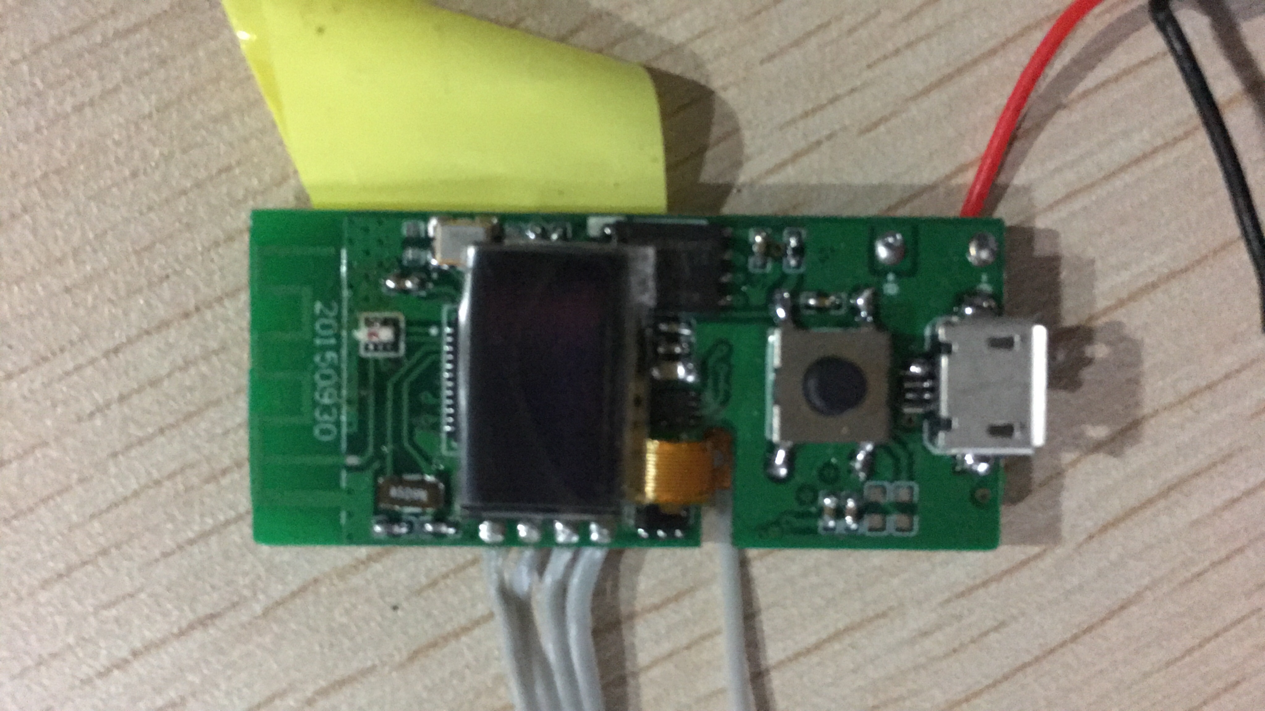
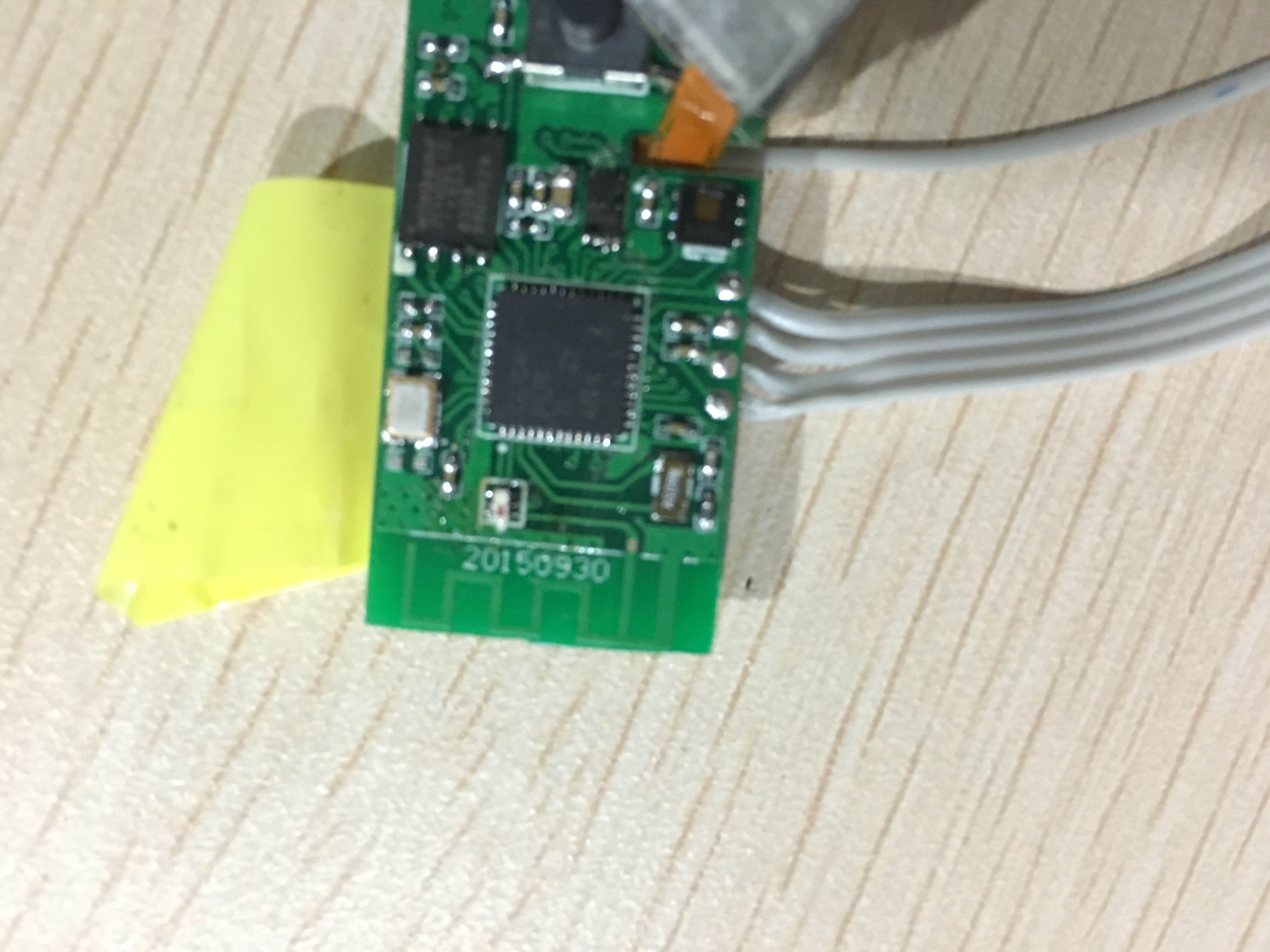
  • Those are very weak signals, that signal levels you could expect to receive on a SMA connector with no antenna mounted (i.e. close to the sensitivity limit). Please take a picture of your HW setup and a close up (really close with as much details as possible) of the module (so that we can see the antenna and mounted components in the RF path).
  • Hi 

    Please see the RSSI output using SmartRF Studio attached for various TX powers. I will get back to you shortly with the details regarding our Antenna design and the 0 Ohm resistor. Also please let me know if this helps.

    ThanksRSSI.doc

    Vikas

  • Hi Eirik

    Sorry for the delay I just received the photos you requested of the close up view of the circuit board. I have attached them to this post. Please review and let me know if this helps debug the issue. 


    Thanks

    Vikas 

  • Hi Eirik 

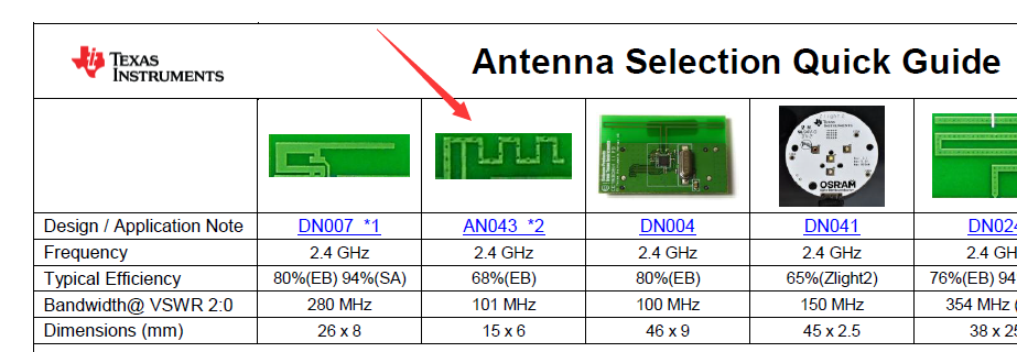
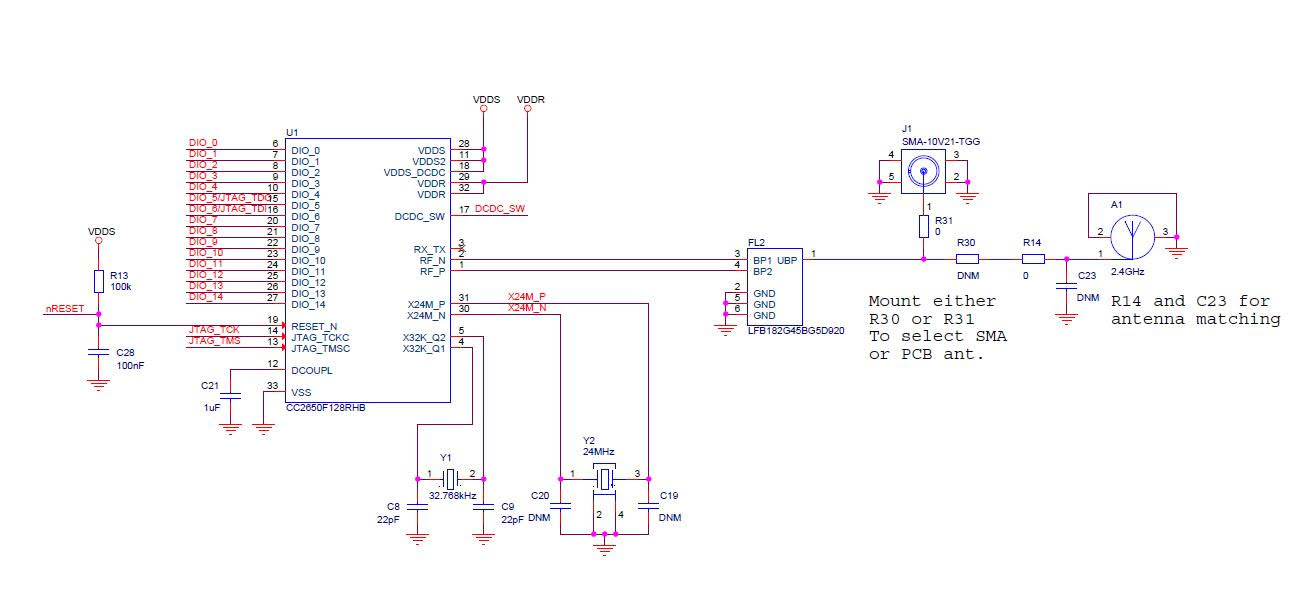
    Please see further details regarding the Antenna as well as which design we are using, attached .

    Thank  CC2650EM-MurBalun_1_0_Assy.pdf8203.CC2650EM-MurBalun_1_0_1_Schematic.pdfs
    Vikas

  • Hello,
    You might have some mismatch towards your antenna?
    Have you checked the impedance of your antenna?

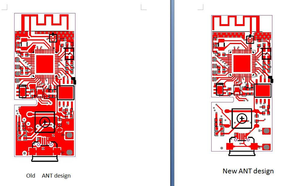
    Its hard to see all the details of the board. It would be easier to review the layout files instead. You should have ground on each side of the single ended RF trace between the BalUn and antenna. You should also move the BalUn closer to CC2640 if possible. Then you can mirror the antenna and place the feed point on the top right side instead to avoid having the RF trace in parallel with the 32 kHz XTAL lines.

    There is a lot of information on the wiki ti.com/ble-wiki:
    processors.wiki.ti.com/.../CC26xx_HW_training_Layout_Considerations.pdf
    processors.wiki.ti.com/.../CC26xx_HW_Checklist
    processors.wiki.ti.com/.../CC26xx_HW_training_RF_Frontends_and_Antennas.pdf
  • Hi Eirik

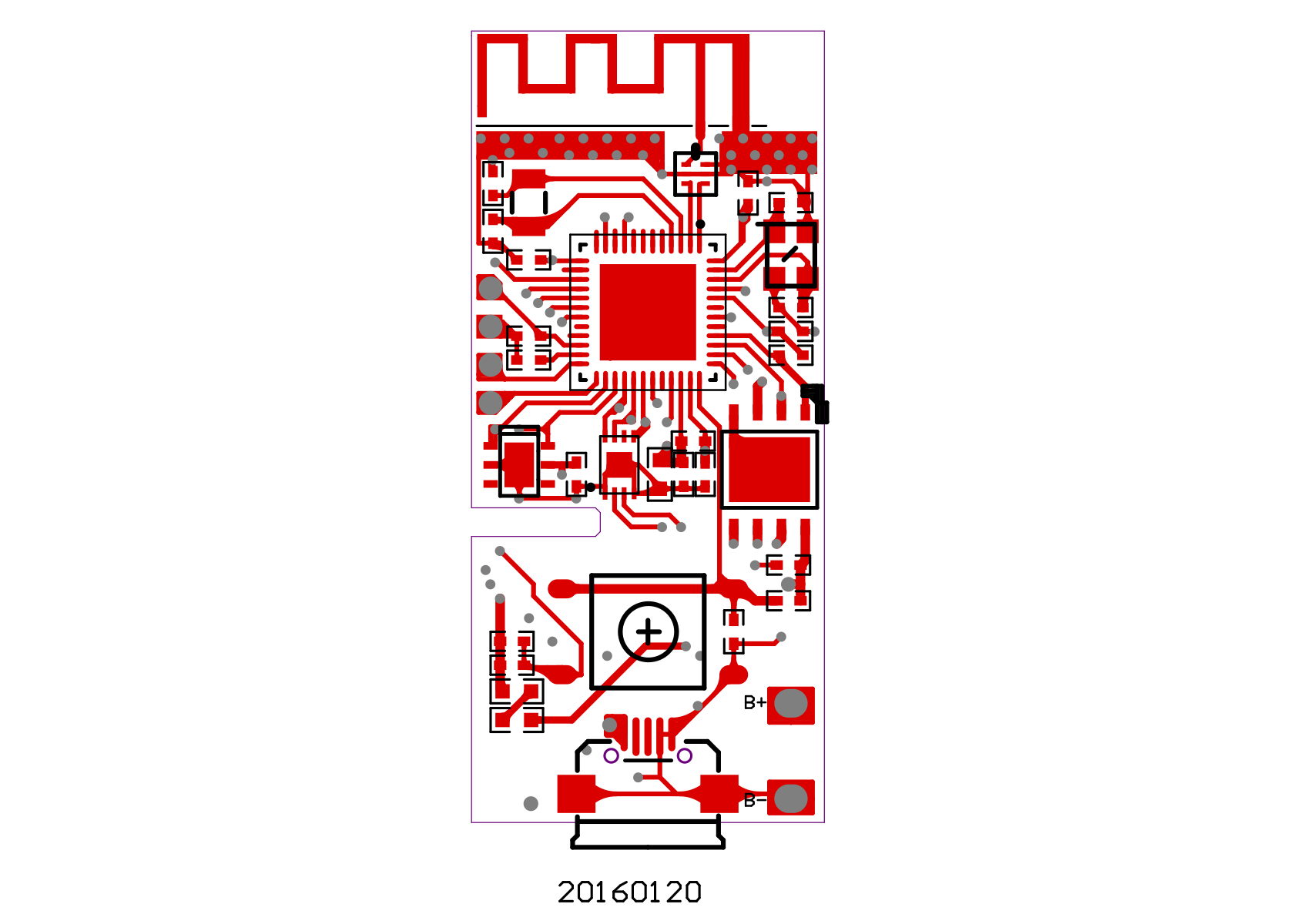
    Please see the detailed PCB Design you requested. We updated our Antenna design, the new design is for a 4 layer PCB board with a thickness of 1mm. Please review and let me know if you see any issues or if you think this design update may help address the problem. 


    Thanks
    Vikas

  • Hello Vikas,
    This looks better. Also remember to make sure the ground plane is poured. It is specifically important that there is direct ground connection between the antenna and ground pad of the device (layer below BalUn and RF path).

    The antenna might be slightly offset from 50 Ohm, but if you followed the reference design closely you should be in the ballpark. If you move the BalUn even closer to the RF pins you have room to add a simple L matching network. But to tune up the antenna you will need access to a network analyzer.

    Some comments:
    - Place the 100 nF cap closer to the VDDR pin (45) before the VIA.
    - Make sure to have the 24MHz XTAL lines as symmetrical as possible.
    - Is the capacitor connected to DCOUPL (pin 23) connected to ground properly?
  • Hi Eirik

    Thank you very much for the response, I will review the recommendations and make the appropriate changes.

    Thanks

    Vikas 

  • Hi Eirik

    Please review the final design for our PCB layout and antenna design and please let me know if you there are any issues that need to be addressed before going to prototyping. As mentioned the primary concerns are getting the maximum signal strength from the CC2640 especially at +5dbm TX. Since its time sensitive can you please get back to us as soon as possible, we really appreciate your help.

    2627.BLE41V3160223A.pdf

  • Hi,
    I looked at the design (but it is very hard to see the different layers, gerber files would be easier). So I am assuming that layer two is only used for a ground layer. I further assume that you have plenty of GND vias underneath the CC2640 chip. I see that you have not added comp for antenna tuning but that this has been discussed with Eirik previously.
    All RF comp, crystal GND pads, the decouple pin and decoupling comp should have separate vias to GND so I would add more GND vias in your design. The decoupling needs to be close to the pin it is to decouple (not the case for pin 45. The DCDC comp on pin 33 needs to be close to the pin and even more important is the grounding of the 10 uF cap. I am not sure where they are in your design, but a non-optimal DCDC design will degrade performance a lot.
  • Hi Charlotte/Eirik

    Please see the Gerber files attached. Also FYI this is a 4-layer PCB. Please review and if you provide all edits in bulleted format we would really appreciate that.


    Thanks

    Vikas GerberFiles.zip

  • Hi,

    1. Consider adding placeholders for the antenna (as Eirik mentioned in his initial review. 
    2. All RF comp, crystal GND pads, the decouple pin and decoupling comp should have separate vias to GND so I would add more GND vias in your design. 
    3. The decoupling needs to be close to the pin it is to decouple. This is not the case for pin 45 in your design, for pin 13, 34, 48 the cap can be closer, 
    4. I see now that the DCDC comp on pin 33 are fairly close to the pin. Adding a via and moving them to a different layer introduce some risk, but to me, it looks ok in your design.