This thread has been locked.

If you have a related question, please click the "Ask a related question" button in the top right corner. The newly created question will be automatically linked to this question.

CC2652RB: Question about the maximum input current on the CC2652RB analog inputs

Part Number: CC2652RB

Hi,

Good day.

Our customer working on the CC2652RB and they have the following question:

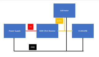
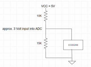
"my question is about the maximum input current on the analog pin of the CC2652RB with VDDS = 3V.
In the current situation it could happen that 5V are applied through a 10K pull up resistor => it means a 2V over voltage (5V-3V) through 10K => 0.2 mA input current. If there is  a symmetrical capability between output and input currents I should expect a limit of 4 mA and in this case 0.2 mA should be a safe current that doesn't exceed the maximum ratings: is it correct?"

Thank you for your usual help. Stay safe always.


Regards,

Cedrick

  • Hi Cedrick,

    I think that should be fine. Table 8.15.6.1 in the datasheet shows the high/low levels for the GPIO pins at 4 mA, so I think it would be safe to give the analog pin 4 mA as well.

    Best,

    Nate

  • Hi Nate,

    Good day. Thank you for your support.

    Our customer provided a feedback on this. Kindly see below.

    "thanks for your reply, however at this point a related question arises:
    With VDDS = 3V, when I apply a source current of 0.2 mA to the analog pin, I can measure 3.4 V on such pin, that I suppose is a limitation effect of the ESD input protection diodes, …
    In the datasheet at paragraph 8.1 “Absolute Maximum Ratings”, “Voltage on ADC input” with voltage scaling enabled, it’s clearly stated that the maximum allowed voltage is VDDS.

    Now if I can source up to 4 mA, the maximum voltage value here reported should be interpreted as “suggested” and not as “absolute maximum ratings” !
    We are producing medical devices and we would be sure that we are not applying excessive stress on the analog input pins in some situations.

    Please could you clarify ?"

    Regards,

    Cedrick

  • Hi Cedrick,

    My apologies, I misunderstood the question. The customer is correct. They should not apply more voltage on the pin than VDDS. 

    Best,

    Nate

  • Hello Nate,

    Thank you for checking this for us.

    I've got a follow up question for our customer regarding this inquiry. We would appreciate your further help on this. Kindly refer to his response below.

    "Many thanks for your reply but I wish to better understand the situation because my opinion is that there’s a lack of information in the datasheet.

    CC2652RB powered at VDDS = 3V.
    Even with 5 microAmps ( 5V through a 400K resistor) at DIO_29 configured as ADC analog input, I can measure 3.4V at this pin.

    Now if Ti in the datasheet simply reports a voltage limit without specifying a current limit, an implicit consequence is that it seems that the device could be stressed or damaged even with 5 microAmps in the ADC input pin !!!

    This is hard for me to understand and I wish to know why: due to direct polarization of input protection diodes that cannot withstand 5 microAmps, avalanche process that may occur, … ?
    For example in the MSP430 family Ti specifies such current: diode input current = +/- 2 mA.

    I wish to receive a thorough answer if possible and not something that is already written in the datasheet.
    "

    Looking forward to your inputs.


    Regards,

    Cedrick

  • Hi Cedrick,

    Thank you for the more detailed message. I think you may be using the device incorrectly or I may not be understanding your setup correctly. What I believe you're telling me is that you are lining a 400K resistor in series with the ADC input, placing 5 V across it, and measuring 3.4 V after the 400K resistor and before the ADC input. In the datasheet it lists the input impedance of the ADC as > 1 MOhm, which makes sense. Based off your calculation (5-3.4 = 1.6V over the 400KOhm resistor -> 0.4 mA  4 uA of current -> impedance of the ADC = input voltage/input current = 3.4V/0.4 mA = 3.4V / 4 uA= 0.85 MOhm (approximating to 1 MOhm)

    This is not the correct way to use your device. You should not be placing a resistor between your source and the device. The device's internal resistance (very high) will govern the amount of current that gets passed into it.

    The correct way to limit your input voltage is with a voltage divider. You can use resistors in the 10kOhm range to attenuate the 5V maximum of the input signal down to the 3V maximum imposed by VDDS. Your parallel resistor must be 1.5X your other resistor to get a 5V signal down to 3V. Lower resistance values will improve your accuracy, but they run the risk of higher currents, whereas higher resistance values are the opposite (more error, less current).

    If you do it this way, the amount of current your device receives should be

    I_total = 5 V / (10000 + (15000 || 850000)) = 202.1 uA

    I_CC2652 = 202.1 uA * 15000/(15000 + 850000) = 3.5 uA.

    While I do not currently have the maximum input current spec for the ADC yet, I have asked internally about it, and I will give it to you at soonest convenience. That being said, I'm highly confident it will be able to handle the 3.5 uA maximum that this system would yield.

  • Hi Nate,

    Good day. Thank you for your detailed reply.

    I've received a response from our customer for this. Kindly refer below.

    "Hello and many thanks for your detailed reply!
    I wish to clarify that it is a test setup configuration in order to verify if even with 4 uA, I can get 3.4V at the ADC input. By the way 1.6V over 400K => 4uA, not 0.4 mA.
    The question is simple: is this situation stressful for the device ?

    If the answer is Yes: I would be very grateful if you can explain me why with 4 uA the device can be stressed without simply saying “because datasheet reports a maximum voltage = VDDS at ADC input”.

    If the answer is No: which is a safe current, 4 uA, 40 uA, 400uA, … ? Moreover in this case it means that datasheet is inaccurate because it’s confusing the ADC operating input voltage, to stay in the linear region avoiding obvious saturation, with Absolute Maximum Ratings.
    May be that for ADC input limits, one must consider what reported two rows above in the same table of AMRs: Voltage on any digital pin, including analog capable DIOs = VDDS + 0.3V ? 

    I wish you a nice day !
    "

    Regards,

    Cedrick

  • Hi Cedrick,

    Thank you for the correction in my calculation.

    I think the issue here is the way the customer is looking at the ADC. The ADC has a voltage applied on it, and from that, it generates a current, not the other way around. The customer should not be sourcing currents deliberately into the ADC pin. Since we impose a limit on the voltage, and the impedance of the ADC is greater than or equal to 1 MOhm, we know that the current will also be limited by this voltage limit. So, as long as your voltage is below VDDS, you current will be safe as well.

    I understand this may be a dissatisfying answer, but I can't really give you a single current number because it will depend on the VDDS used. Say you use a VDDS of 3.3 V, then your current limit will be 3.3V / (Input impedance of the ADC) = 3.3V/1MOhm = 3.3 uA. But this just stems from the voltage limit in the first place. 

    Our validation team has tested the pins up to voltages slightly higher than a 3 V VDDS supply, but they are hesitant to verify it for operation at the VDDS + 0.3 V level due to internal circuitry on the ADC. I'm corresponding with our design team to see if there's any other relevant information about current limits on the ADC and I'll let you know if I learn more, but I really do think this is all you'll need to design effectively and safely.

    Nate