Chatto,
CC2511 USB-Dongle Reference Design 1.3 (Rev. C) (swrc062c) readme file gives copper thickness of 35um, whereas on our board the top layer copper thickness is about 17um (0.5oz copper). We are trying out best not to alter this thickness as this has been proven to work with other high-speed components by providing the right impedance. New change to the existing copper thickness would be risky and expensive.
You mentioned in http://e2e.ti.com/support/low_power_rf/f/155/t/106382.aspx#375099 that balun and filter network has to be changed if the circuit is different from the reference design. We have some questions:
1. Does antenna itself has to be changed?
SWRA117D page 4 said:Information about the PCB can be found in a separate readme file included in the reference design. To compensate for a thicker/thinner PCB the antenna could be made slightly shorter/longer.
However the expression “slightly short/longer” is vague and is not instructive since designer exact information to do the adjustment. How exactly should the shorter/longer mean? Among the various antenna dimension figures, which one do we need to change?
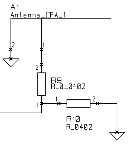
2. AN068 shows a cascading of 1) DC blocking capacitors + 2) balun + 3) Pi filter network. On the other hand, if we use Johanson chip balun 2450BM15B0003, the datasheet shows no DC blocking capacitor nor Pi filter network. So are they all integrated into the chip balun? Please refer to figure below.
Again page 3 of AN043:
SWRA117D page 3 said:The IFA was designed to match an impedance of 50 ohm at 2.45 GHz. Thus no additional matching components are necessary.
What are the “unnecessary matching components” here? We are considering to use a combination of AN043 antenna + Johanson 2450BM15B0003, so would the circuit be as simple as just a Johanson chip balun, preceded by an Johanson L-07C10NJV6 or L-14C10NJV6 inductor, and the directly followed by AN043 antenna?
Thanks and regards,
Matt


