


Hi All,
I have inherited an RF transmitter project which transmits a device ID as a UART, and I have been asked to develop a receiver to detect and display the ID.
The transmitter hardware is already designed and has been in manufacture for some time. It uses the TI CC1070 and is configured to transmit a burst of RF, encoded with the ID in UART mode at 9600 baud every 2 seconds. I have gone through the CC1070 datasheet and have re-written the device configuration table as follows:
rf_table
	retlw 0x81 ;00 MAIN         [Select A, Normal operation, no power down, no reset]
	retlw 0x0A ;01 INTERFACE    Internal Osc, PA_EN enabled and active high
	retlw 0x2D ;02 RESET        Do not write '1's to this register
	retlw 0x00 ;03
	;
	; MET 434.050 approx freq
	;
	retlw 0x3A ;04 FREQ_2A      }
	retlw 0x1F ;05 FREQ_1A      ) FREQ=0x1D0F97, DITHER=1
	retlw 0x2F ;06 FREQ_0A      )
	retlw 0x39 ;07 CLOCK_A      REF_DIV=DIV2, MCLK_DIV1=DIV48, MCLK_DIV2=DIV2
	;
	retlw 0x3A ;08 FREQ_2B      )
	retlw 0x1F ;09 FREQ_2A      ) FREQ=0x1D0F97, DITHER=1
	retlw 0x2F ;0A FREQ_0B      )
	retlw 0x39 ;0B CLOCK_B      REF_DIV=DIV2, MCLK_DIV1=DIV48, MCLK_DIV2=DIV2
  ;
	retlw 0x44 ;0C VCO_CUR      Both VCO_CURRENTs = 2.8mA
	retlw 0x03 ;0D MODEM        UART mode, DCLK=1
	retlw 0x9B ;0E DEVIATION    TX_SHAPING=1, TXDEV_X=1, TXDEV_M=11
	retlw 0x00 ;0F
	retlw 0x00 ;10
	retlw 0x00 ;11
	retlw 0x00 ;12
	retlw 0x00 ;13
	retlw 0x00 ;14
	retlw 0x20 ;15 LOCK         LOCK_SELECT=Cont, WINDOW_WIDTH=0, LOCK_MODE=0, LOCK_ACCURACY=0
	retlw 0x00 ;16
	retlw 0x07 ;17 ANALOG       402-470MHz band, PD_LONG=0, PA_BOOST=1, DIV_BUFF_CURRENT=3
	retlw 0x04 ;18 BUFF_SWING   PRE_SWING=0, TX_SWING=4
	retlw 0x02 ;19 BUFF_CURRENT PRE_CURRENT=0, TX_CURRENT=2
	retlw 0x93 ;1A PLL_BW       PLL_BW=147
	retlw 0x3C ;1B CALIBRATE    CAL_START=0, CAL_DUE=0, CAL_WAIT=3, CAL_SELECT=1, CAL_ITERATE=4
	retlw 0x0F ;1C PA_POWER     PA_HIGH=0, PA_LOW=15
	retlw 0x00 ;1D
	retlw 0x00 ;1E
	retlw 0x00 ;1F
	retlw 0x00 ;20 POWERDOWN    All systems powered up
Using a handheld receiver, I can confirm that the transmitter is sending an RF burst every 2 seconds.
I have constructed a receiver using a microcontroller module connected to a cc1020mx module from a TI development kit, and have converted the -868MHz RF circuit to -433MHz, (values optimised for 434.050MHz using SmartRFStudio). I configure the CC1020 as follows:
                          // MAIN         set by cc1020_reset
  spi_write(0x01, 0x0F);  // INTERFACE    int osc, DIO output, set PA and LNA control
                          // RESET        should be read only
  spi_write(0x03, 0x8F);  // SEQUENCING   PSEL power up, min RX_WAIT, max CS_WAIT
  spi_write(0x04, 0x3A);  // FREQ_2A      )
  spi_write(0x05, 0x1F);  // FREQ_1A      ) FREQ = 0x1D0F97
  spi_write(0x06, 0x2F);  // FREQ_0A      )
  spi_write(0x07, 0x39);  // CLOCK_A      REF_DIV=DIV2, MCLK_DIV1=DIV48, MCLK_DIV2=DIV2
  spi_write(0x08, 0x3A);  // FREQ_2B      )
  spi_write(0x09, 0x1F);  // FREQ_1B      ) FREQ = 0x1D0F97
  spi_write(0x0A, 0x2F);  // FREQ_0B      )
  spi_write(0x0B, 0x39);  // CLOCK_B      REF_DIV=DIV2, MCLK_DIV1=DIV48, MCLK_DIV2=DIV2
  spi_write(0x0C, 0x44);  // VCO          Both VCO_CURRENTs = 2.8mA
  spi_write(0x0D, 0x53);  // MODEM        ADC_DIV=DIV12, PN9 disabled, UART mode
  spi_write(0x0E, 0x9B);  // DEVIATION    TX_SHAPING=1, TXDEV_X=1, TXDEV_M=11
  spi_write(0x0F, 0xC6);  // AFC_CONTROL  SETTLING=3, RXDEV_X=0, RXDEV_M=6
  spi_write(0x10, 0x2F);  // FILTER       FILTER_BYPASS=0, DEC_SHIFT=1, DEC_DIV=DIV16
  spi_write(0x11, 0x61);  // VGA1         CS_SET=1, CS_RESET=1, VGA_WAIT=0, VGA_FREEZE=1
  spi_write(0x12, 0x55);  // VGA2         LNA2_MIN=0, LNA2_MAX=1, LNA2_SETTING=1, AGC_DISABLE=0, AGC_HYST=1, AGC_AVG=1
  spi_write(0x13, 0x2F);  // VGA3         VGA_DOWN=1, VGA_SETTING=31
  spi_write(0x14, 0x2D);  // VGA4         VGA_UP=1, CS_LEVEL=13
  spi_write(0x15, 0x20);  // LOCK         LOCK_SELECT=Cont, WINDOW_WIDTH=0, LOCK_MODE=0, LOCK_ACCURACY=0
  spi_write(0x16, 0x78);  // FRONTEND     LNAMIX_CURRENT=1, LNA_CURRENT=3, MIX_CURRENT=1, SDC_CURRENT=0, LNAMIX_BIAS=0
  spi_write(0x17, 0x47);  // ANALOG       402-470MHz band, LO_DC=1, VGA_BLANKING=0, PD_LONG=0, PA_BOOST=1, DIV_BUFF_CURRENT=3
  spi_write(0x18, 0x14);  // BUFF_SWING   PRE_SWING=0, RX_SWING=2, TX_SWING=4
  spi_write(0x19, 0x22);  // BUFF_CURRENT PRE_CURRENT=0, RX_CURRENT=4, TX_CURRENT=2
  spi_write(0x1A, 0xAF);  // PLL_BW       PLL_BW=175
  spi_write(0x1B, 0x34);  // CALIBRATE    CAL_START=0, CAL_DUE=0, CAL_WAIT=3, CAL_ITERATE=4
  spi_write(0x1C, 0x0F);  // PA_POWER     PA_HIGH=0, PA_LOW=15
  spi_write(0x1D, 0x00);  // MATCH        RX_MATCH=0, TX_MATCH=0
  spi_write(0x1E, 0x00);  // PHASE_COMP   PHASE_COMP=0
  spi_write(0x1F, 0x00);  // GAIN_COMP    GAIN_COMP=0
  spi_write(0x20, 0x00);  // POWERDOWN    All systems powered up
I call the initialisation routing and check for lock, (by reading the STATUS register (0x40)). STATUS returns not locked the first read after calibration, but thereafter returns 0xB2 or 0xB3, which seems to indicate it's locked successfully.
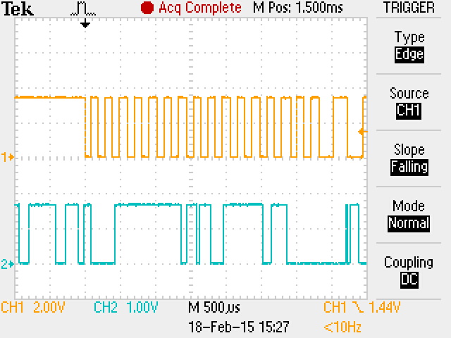
The image below shows the data sent to the DI pin of the CC1070 (top trace, yellow), and received at the DIO pin of the CC1020 (bottom trace, blue). As you can see, there is no discernible correlation between the data sent and the data received. Indeed, the received data looks like random bit transitions, as if the receiver is not receiving the transmitted signal.
I'm about out of ideas now, and RF is not my strong field. So if anyone has any suggestions, I'd really appreciate that. Many thanks in advance.

