Because of the Thanksgiving holiday in the U.S., TI E2E™ design support forum responses may be delayed from November 25 through December 2. Thank you for your patience.

This thread has been locked.

If you have a related question, please click the "Ask a related question" button in the top right corner. The newly created question will be automatically linked to this question.

CC1101 design validation

hi,

after 5 non-functional modules (4 not emitting/receiving and 1 not responding), i decide to make new desing.

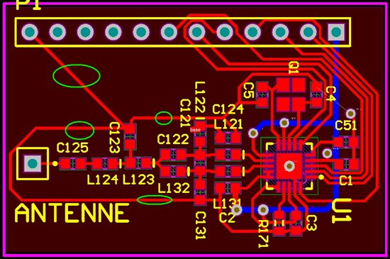
here is my new desing, can you tell me what you think about this design ?

it is 868Mhz version.


schema : http://demo.ovh.com/download/4cea955300692df7e4fd5d0be106b15f/base.pdf

PCB : http://demo.ovh.com/download/4cea955300692df7e4fd5d0be106b15f/desing.jpg
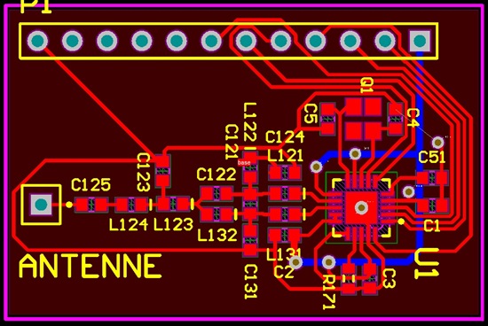
PCB have GROUND plane on both side (not presented here).

thanks,

marc


  • Is the schematic value of L132 correct ? - This should be 18nH.

    //Richard.

  • oups, thanks for this error.

    the desing looks good ?


  • Marc, 

    You wrote that ground was on two layers that are not shown. To perform a visual inspection of a layout estimating the performance of the ground plane is very important.

    From just looking at the picture you have included, it seem that "ground" has been routed as a trace on the top surface along with the remaining signals, see the traces I highlighted in green. This approach will not work, you need an actual ground plane and then have lots of small vias connecting various points on the circuit that need ground to it.

    Please post a complete image of all the layers that you would like to have a review of.

    Regards,
    /TA 


  • thanks for your help.

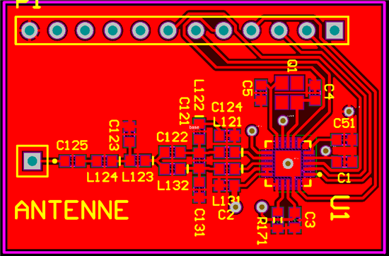
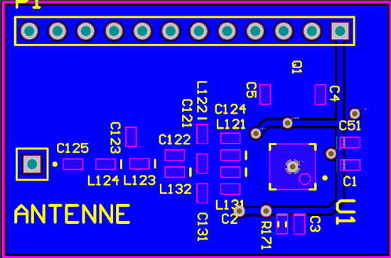
    here is desing with ground plane :

    top :


    bottom :


    thanks,

    marc


  • Marc,

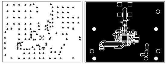
    Your ground planes look ok, but there is not enough ground to ground vias. If you take a look at the reference design found www.ti.com, you will find that we use a lot of vias to minimize the inductance between ground layers and also add more vias in critical sections. Critical sections are decoupling caps, tuning caps for the XTAL and very critical ones are the components in the RF section that are attached to ground.

    I have not counted the number of vias on this design, but it likely close to 100. The PCB size is 3x4cm. If you chose not to copy our reference design I recommend that you take a close look at where we have ground vias and apply similar strategy on your design.

    Regards,
    /TA@LHR