This thread has been locked.

If you have a related question, please click the "Ask a related question" button in the top right corner. The newly created question will be automatically linked to this question.

Re:CC2545 AHDSP

Other Parts Discussed in Thread: CC2545, CC2544, Z-STACK, CC2538, CC2541, CC2540, CC2592, CC2590, CC2530

Hi all,

Kindly provide the information for the following query.

I want to built a network with 4 CC2545 devices(say for example) in which one will be the receiver and remaining 3 will be the transmitters. So simply it is a Many to one communication. Is it possible to bind 3 devices with one device in this fashion with CC2545.

Also kindly provide about the time synchronization achieved in this AHDSP when multiple devices are there.

Note: For the above two query's the information given in application Report is not sufficient. Kindly provide information other than this document.

Regards,

N.vamsi


  • N.vamsi,

    We do not more examples that what is already on the web. What is AHDSP?

    Regards,
    /TA

    Software (3)

    CC2543 mini-BLE Broadcaster  (ZIP 414 KB )    675 views, 09 Jul 2014  
    CC254x Proprietary Mode Packet Error Rate Test (Rev. B)  (ZIP 232 KB )    715 views, 30 Apr 2013  
    CC2541/43/44/45 Peripherals Software Examples  (ZIP 763 KB )    3,333 views, 24 Oct 2012  
  • Hi all,

    Thank you for giving reply.

    AHDSP means "AUTONOMOUS HIGH DENSITY STREAMING PROTOCOL".

    Regards,

    N.vamsi

  • Ahh,

    I am the author of this application note, the protocol is based on sniffing the "master time slot" packet timing and then scheduling its own packets around this. At 250kbps, you will get +/-1 symbol timing at 250kbps, so 1/250000 = 4us, at 500kbps it becomes 2us and at 1mbps it becomes 1us.

    You should be able to pretty easily modify this example code to become a one to many type protocol and not many point to point protocols.

    Regards,
    /TA
  • Hi Dear,

    Thank you for your reply.

    We have following Query's  regarding CC2545 Chip.

    1.What are the possible ways of pairing that can be achieved using these CC2545 chips. [i.e like 1. one to one only   2. One transmit can send data to multiple receivers etc..]

    2.In our application we simply need to transfer the Data from one transmitter to multiple receivers. Is it possible to achieve this fashion using CC2545 or not?

    3.If above fashion is possible then let us consider i have 4 CC2545 Chips. Among them I configured 1 Chip as transmitter and remaining 3 as receivers then Kindly mention the parameters i need to configure in those modules[Like Whether ID's should be same for all modules or not etc..].

     4.In this case how the time slot allocation will be done to 4 modules in real time sense[Means Will it be 1st minute of every one hour or First second of every minute etc..].

    Kindly respond as early as possible.

    Regards,

    N.vamsi.

  • N.vamsi,

    You wrote:

    1.What are the possible ways of pairing that can be achieved using these CC2545 chips. [i.e like 1. one to one only   2. One transmit can send data to multiple receivers etc..]

    • The CC2545 is a basic 2.4GHz RF SoC, you can write any software on there to achieve any type of network you want. The AHDSP protocol is optimzed for many concurrent point to point links. But it should be pretty easy for you to take that base code and modify it to become a one to many type protocol.

    2.In our application we simply need to transfer the Data from one transmitter to multiple receivers. Is it possible to achieve this fashion using CC2545 or not?

    • Yes, but we do not have software that shows that out of the box.

    3.If above fashion is possible then let us consider i have 4 CC2545 Chips. Among them I configured 1 Chip as transmitter and remaining 3 as receivers then Kindly mention the parameters i need to configure in those modules[Like Whether ID's should be same for all modules or not etc..].

    • We do not have code examples for this particular use case avaiable.

    Regards,
    /TA

  • Dear Sir,

    Thank you for your earlier reply.

    1.Kindly share the Code for Point to point Communication. Also kindly provide the Software or any other documentation available regarding the Point to Point Communication[regarding "process of initiation and establishment of communication" etc..].

    2.As per your application report are the terms Frame length, Time slot are configurable are not? [Which basically depends on the number of devices going to be used in the particular application]. Here the main intension is to know up to what time period a particular chip can transmit the data in its own time slot.

    3.In TDMA let us consider there are 4 modules. In those 2 are configured as Receivers and 2  as transmitters. Now is there any Fixed pattern of Time slot and frequency allocation like after allocation of some 7 time slots(as indicated in page no 3 in application report) only in a particular frequency[say 2402 MHZ] the next frequency[say 2403 MHZ] should be allocated or not.

    If not Kindly provide information regarding the Pattern in which time slot and frequency will be allocated for the 4 CC2545 Chips in above application.

    Awaiting for your earlier reply.

    Regards,

    N.vamsi.

  • Dear Sir,

    1.Could you please share the Code for Point to point Communication. Also kindly provide the Software or any other documentation available regarding the Point to Point Communication[regarding "process of initiation and establishment of communication" etc..]. 

    Regards,

    Manikanta.K

  • Manikanta, 

    The code is already released on the web.

    Regards,
    /TA

  • Hi sir,

    Thank you for your earlier reply,

    Kindly provide the solution for the following query sir:

    1 .Could you provide the brief explanation regarding how the communication(Process) established between two devices (point to point communication).

    2.As per your application report are the terms Frame length, Time slot are configurable are not? [Which basically depends on the number of devices going to be used in the particular application]. Here the main intention is to know up to what time period a particular chip can transmit the data in its own time slot.

    3.In TDMA let us consider there are 4 modules. In those 2 are configured as Receivers and 2  as transmitters. Now is there any Fixed pattern of Time slot and frequency allocation like after allocation of some 7 time slots(as indicated in page no 3 in application report) only in a particular frequency[say 2402 MHZ] the next frequency[say 2403 MHZ] should be allocated or not.

    If not Kindly provide information regarding the Pattern in which time slot and frequency will be allocated for the 4 CC2545 Chips in above application.

    Regards,

    Manikanta.K

  • Hi Sir,

    1.I mean that Brief explanation  means what are the steps we have to follow for the configuration of a module as Transmitter and receiver? and In what pattern time slots and frequency slots are allocated for those module.

    Awaiting for your Reply,

    ----------------------------------

    Manikanta.K


  • Hi Sir,

    1.I mean that Brief explanation means what are the steps we have to follow for the configuration of a module as Transmitter and receiver? and In what pattern time slots and frequency slots are allocated for those module.

    Awaiting for your Reply,

    ----------------------------------

    Manikanta.K
  • Hi Sir,

    1.I mean that Brief explanation  means what are the steps we have to follow for the configuration of a module as Transmitter and receiver? and In what pattern time slots and frequency slots are allocated for those module.

    2.If any stack is available to download  into CC2545?please share the stack sir.

    Awaiting for your Reply,

    ----------------------------------

    Manikanta.K

  • Manikanta, 

    In the zip file on our website (swra433.zip) there is a small excel spreadsheet that helps you calculate what is possible.

    you type in values into the 5 (highlighted in orange) fields and then it will tell you in the configuration is possible.

    Then you type into the main c file (see below) the configuration that you need.

    Regards,
    /TA

    /******************************************************************************
    * System configurations
    *
    * This sections defines the starting conditions of the TDMA code. In a final
    * product one could implement a system in which the settings are transmitted to
    * the product using a bootup process, but to keep things simple here we have
    * decided to demo using a fixed starting condition.
    *
    * The code first jumps into Loopback mode where you can demostrate the sending
    * UART data back and forth, this automatically times out and the code continues
    * into the "Auto start settings" as defines in the define. This is controled by:
    *
    * cRfState = STATE_LOOPBACK;
    * cRfState_auto = STATE_INIT_RX; // initial state of statemachine
    *
    * The next setting is the start and stop frequencies the software is allowed to
    * operate accross, this is usefull for passing regiounal regulatory requirements
    *
    * cRfFreqStart = 23; // 2379+Fword (2379+23) = 2402
    * cRfFreqStop = 103; // 2379+Fword (2379+23) = 2482
    *
    * The base datarate of the system can be changed. Carefull considderation should
    * be taken as this influences many system aspects at the same time. The most
    * important one is adjacent channel intefererence.
    *
    * cRfMod = MSK_500kbps; // see table below for options
    *
    * GFSK_250kbps_160khz, GFSK_1Mbps_160khz, GFSK_1Mbps_250khz, GFSK_2Mbps_320khz,
    * GFSK_2Mbps_500khz, MSK_250kbps, MSK_500kbps
    *
    * This variable defines the Frametime in milliseconds, this is the time allocated
    * to cycling thru the entire table of concurrent users (cRfNusers)
    *
    * cRfFtime = 50; // Frametime in milliseconds (1-65535)
    *
    * The number of concurrent users that can be allocated on a single channel, this
    * defines the number of TDMA time slots used in the system.
    *
    * cRfNusers = 8; // Number of timeslots per frame (1-16)
    *
    * The defines the Unique 32 BIT ID for each of the pair of nodes that need to
    * find each other and commmunicate.
    *
    * cRfid[4] = {0x12, 0x34, 0x56, 0x78}; // 32 bit ID
    *
    * The variable defines the amount of payload the system will carry in each direction.
    * The upper limit is defined by the FIFO depth minus the system overhead. (128-13=115)
    *
    * cRfForwardlength = 32; // amount of payload in forward link
    * cRfReverselength = 32; // amount of payload in reverse link
    *
    * The variable is meant to be able to set the maximum power of the each of the nodes
    * this has not been implemented fully.
    *
    * cRfPower = 20; // 20dBm output is maximum down to 0
    *
    * Timer resolution, this sets the resolution of the timer.
    *
    * cRfTimerRes = 10; // 10 => 1000/10 = 100us resolution
    *
    ******************************************************************************/
    unsigned char cRfState = STATE_LOOPBACK; // initial state of statemachine
    unsigned char cRfState_auto = STATE_INIT_TX; // initial state of statemachine
    unsigned char cRfFreqStart = 23; // 2379+Fword (2379+23) = 2402
    unsigned char cRfFreqStop = 103; // 2379+Fword (2379+23) = 2482
    unsigned char cRfMod = MSK_500kbps; // see above table
    unsigned int cRfFtime = 50; // Frametime in milliseconds (1-65535)
    unsigned char cRfNusers = 8; // Number of timeslots per frame (1-16)
    unsigned char cRfid[4] = {0x12, 0x34, 0x56, 0x78}; // 32 bit ID
    unsigned char cRfForwardlength = 32; // amount of payload in forward link
    unsigned char cRfReverselength = 32; // amount of payload in reverse link
    unsigned char cRfPower = 20; // 20dBm output is maximum down to 0.
    unsigned char cRfTimerRes = 10; // 10 => 1000us/10 = 100us resolution

  • Hi sir,

    Thank you sir for your earlier reply,

    Kindly provide the solution for the following query.

    1.By keeping loop back state is it mandatory to keep the initial state as RX.?

    2.I had  2 CC2545 Chip I want to keep one as Transmitter and other as Receiver the above configurations are sufficient to the 2 chips or not?

    3.Another one was Antenna Selection?Could you please provide the process for Antenna Selection?

    4.For this CC2545 which Antenna was Preferable ?

    5.Actually In the zip file (swra433.zip) in web site,there was a one example code usb_tdma_trx_130718 .

    It was CC2544 Chip Based example.

    Is there any stack is readily available for CC2545 chip?like( Z-stack for CC2538)   (or) Example Code for CC2545 Chip for basic testing is RF link was establishing between two devices  or not?

    Regards,

    Manikanta.K 

  • Thank you sir for your earlier reply,

    Kindly provide the solution for the following query.

    1.By keeping loop back state is it mandatory to keep the initial state as RX.?

    • No, the two choices are: STATE_INIT_RX, STATE_INIT_TX
    • If you compile one chip with STATE_INIT_RX and the other with STATE_INIT_TX and they have the same ID, they will connect.

    2.I had  2 CC2545 Chip I want to keep one as Transmitter and other as Receiver the above configurations are sufficient to the 2 chips or not?

    • yes, 2 device is all that is required.

    3.Another one was Antenna Selection?Could you please provide the process for Antenna Selection?

    • It depends on what you care about, size, performance, cost.

    4.For this CC2545 which Antenna was Preferable ?

    • In my opinion the best antenna design we have is

    5.Actually In the zip file (swra433.zip) in web site,there was a one example code usb_tdma_trx_130718 .

    • Yes, correct we used the USB version for this project. I am not aware of a stack that runs out of the box on the CC2545. You should be able to adopt SWRA433 to remove the USB.

    Regards,
    /TA

  • Hi sir,

    Thank you for your earlier reply.

    1.By removing the USB part in existing code ,we can use it for basic testing of RF link between two devices or not?

    Regards,

    Manikanta.k

  • Yes, the code blinks a couple of LED's so you might want to adapt the ports to your specific hardware.

    Regards,
    /TA
  • Hi sir,

    Thank you sir for your earlier reply.

    1.Could you please share the schematic regarding Interfacing Antenna Circuit to this CC2545 Chip if there is possible?

    2.Kindly share the tools like Code loading and Sniffer tool and Sensing commands manually through Exes like Radiocrafts.

    3.Prefer the On-chip antenna for this CC2545 Chip sir?

    Regards,

    Manikanta.K

  • Hi sir,

    Kindly provide the solution for the following queries:

    1.Kindly share the code loading procedure to this CC2545 Chip.

    2.Kindly share the tools like Code loading and Sniffer tool and Sensing commands manually through Exes like Radiocrafts.

    3.Prefer the On-chip antenna for this CC2545 Chip sir?

    Regards,

    Manikanta.K
  • Manikanta, 

    1) I used IAR () for code development and debug

    2) Sniifer tools I used 

    3) This depends on what your system requirements are, I suggest starting by copying when we did, which was a PCB antenna and then if it does not have enough performance or the size is not right then contact a chip antenna manufacture to help you select the right antenna for your needs. We have good selection guide here :

    Regards,
    /TA 

  • Hi sir,

    Thank you for your earlier reply..

    1.could you please provide the detailed explanation about code loading process.

    Regards,

    Manikanta. K

  • Manikanta,

    Please have a look at the hardware user guide for the CC2540/CC2541 series devices. They use the same tool chains.

    Look at section 5 "Programming / Debugging the CC2540 or CC2541" in

    www.ti.com/.../swru270c.pdf

    Regards,
    /TA
  • Hi sir,
    Thank you Sir for your quick response sir,
    Regards,
    Manikanta. K
  • Hi Sir,

    1.We can use CC2592 Power extender to this CC2545 Chip or not?

    2.If it is possible could you please explain it sir?

    Regards,

    Manikanta.K

  • Yes you can. I recommend looking at this post, e2e.ti.com/.../444711 for guidelines.
  • Hii sir,

    Thank you for your earlier reply.

    Kindly provide the solution for the following query:

    1)I had the 2 cc2545 devices I want to establish the communication between those two devices.could you please provide the example code for test the RF link between those two devices.(like one device as transmitter and other was receiver).

    Awaiting for your reply,

    Regards,

    Manikanta.k

  • I suggest that you start with the PER test available on the CC2545 web page www.ti.com/.../toolssoftware
  • Hi sir,

    Thank you for your earlier reply.

    What do you mean that PER test?

    Regards

    Manikanta. K

  • The PER test is a SW example available on the web that sets up a link between the two devices.
  • Hii sir,
    Thank you sir for your earlier reply.
    Kindly please share the procedure of that test by the by I didn't found software in cc2545 page.
    Could you please send the link where software was available
    Regards,
    Manikanta. K
  • Look under the SW folder or try this link

  • Hi sir,

    Thank you for your earlier reply.

    I found the hex files for cc254x series for per test.

    I had already the 2 pcb boards with cc2545 and cc 2592 power extender. Now could you please share what the process I follow

    To do this per test.

    Regards

    Manikanta. K

  • Hi sir,

    Thank you for your earlier reply,

    1.I think it was useful to do the PER test for CC2545 evaluation modules. But i need to test the CC2545 Chips. For that I designed the board for CC2545 Chip with

    CC2592power extender. Is any ready stack is available to load into the cc2545 Chip and to test it.(like one as transmitter and one as receiver).If it is available, kindly

    share those files sir.

    Regards,

    Manikanta.k

  • Hi sir,
    Thank you for your earlier reply.
    1.I think this files will useful to do PER test for CC2545 Evaluation modules. But I want to test the CC2545 Chips.For that I designed a PCB for CC2545 Chip with CC2592 Power extender. Is there ready stack(like CC2538 stack)is available or not to load into the CC2545 Chip to test it.
    If it is available kindly share the files sir.
    Regards,
    Manikanta.K
  • I suggest you have a look at the CC2540 CC2590 design www.ti.com/.../swra422.pdf and see how they control the range extender and add this to the code you use for testing .
  • Hi Sir,

    Thank you for your earlier reply.

    1.Could you give confirmation to me sir,Now I have to add the controlling of power extender code to the PER test code.With this I can do the testing.

    2.For confirmation Iam saying my requirement once again sir.

    I want to test the RF link between two cc2545 chips.For this I designed the hardware with cc2592 power extender.I want to check one as transmitter and receiver .Is receiver receives the data from transmitter or not sir?

    Could you please give guidelines as in the direction of firmware sir.(Like code for Transmitter and receiver )

    Regards,

    Manikanta.K

  • Yes, you have to add control signals to the range extender depending on your design. You can also look at the user guide for the correct settings, www.ti.com/.../swru283b.pdf.

    Another option for testing would be using SmartRF studio. You will still need to set the control signals but it requires less coding than changing the PER test code.
  • Hi sir,
    Thank you for your earlier reply.
    Regards,
    Manikanta.k
  • Hi sir,

    Kindly provide the solution for the following query sir:

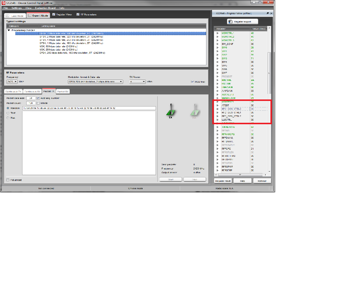
    1)Previously I was discussed with you regarding the I designed a PCB with CC2545 chip and CC2592 Power extender. For basic RF link testing you said that choose Smart RF studio tool. please observe the following PIC. IN RF parameters section there is no choice for selection of range extender .It is available for CC2530 device. Is smart RF studio will work or not when CC2592 mount with CC2545 ?

    2)Could you please provide the example code for the CC2545 chip to do the basic RF link test between two devices rather than which was available in the ti site.

    the code available in the swra433 zip file was cc2544 device.so please send the code other than that.

    Awaiting for your Reply,

    Regards,

    Manikanta.K

  • Manikanta, 

    The only example code we have is what CHS provided a link to in the the first reply at the top of this conversation. We have no other software available for you and we are not planning on making any more examples.

    Regards,
    /TA

  • Hi sir,

    Thank you for your quick response sir.

    I was asked for just information.

    Regards,

    Manikanta.K

  • Hi sir,

    Kindly provide the solution for the following query sir:

    1)I was connected control signals of  Power extender cc2592  to cc2545 as follows:

    PA_EN to P0_1

    LNA_EN to P0_0

    HGM to P2_0

    with this connections  I can do the basic RF link test with smart RF studio or not?

    Regards,

    Manikanta.K

  • yes, you can test it, but you need to set the IO your self in the register view window on the right side of the device panel. How to control the IO pins is described in the user guide, and you can use how it is done in this app note www.ti.com/.../swra422.pdf as a reference (in the app note they use other IO pins, the CC2541 and CC2590 but the principals are the same.
  • Thank you sir for your earlier reply.

    1.we can connect the control signals of CC2592 power extender to the any 3 GPIO pins of CC2545. or not?

    2.In device control panel of CC2545 there is no choice for range extender.Still I can do the test or not?

    3.Could you please share the document regarding algorithm or flowchart of PER test code for step by step process and initialization purpose.

    Regards,

    Manikanta.K

  • T2) yes, but you have to set the IO pins manually in the register view on the right side of the device panel, see the user guide for which pins and reg settings

    3) Set the control signals for the CC2592 according to the state of the CC2545 (RX/TX/ power down) and it works.

    Good luck. 

  • Thank you sir for your quick response.
    1.By doing the modification regarding control signals of power extender in PER test code which was available in the site will be sufficient or not.
    please give the confirmation sir.
    Regards,
    Manikanta.K
  • Hi sir,

    Kindly provide the solution for the following query:

    1.Could you please explain how the communication establishment between cc2545 chips an how the CC2545 chip behaves in the following cases :

    A)Point to point communication(one as transmitter and one as receiver)

    B)In this case there are 3 cc2545 chips, one was receiver and two are  transmitters.(many to one communication)

    C)In this case there are 3 cc2545 chips, one was transmitter and two are receivers.(one to many communication)

    please provide the Step by step process and brief explanation for the above cases.


    Awaiting for your reply,

    Manikanta.K

  • We have provided you with all the solutions we have available. These should give you a good starting point, it is up to you to alter to fit your specific application. I am sorry, but we do not have anything more available nor is this planned. Good luck!
  • Hi sir,

    To clear my ambiguities  I was asked how the cc2545 behaves or communication process steps(means data travel path) in the 3 types of communications.

    if it is available please post the answer sir. or not.

    else provide the data travel path for point to point communication(2 devices 1 was transmitter and 2 was receiver) if we interface the power amplifier to the cc2545 chip.

    Thank you for your cooperation up to now.

    Regards,

    Manikanta.k

  • I am sorry, I do not understand what you are asking for (data travel path?). Further we do not have any more info than what we have already provided.