This thread has been locked.

If you have a related question, please click the "Ask a related question" button in the top right corner. The newly created question will be automatically linked to this question.

Long distance between NFC antenna and NFC IC

Hi,

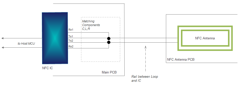
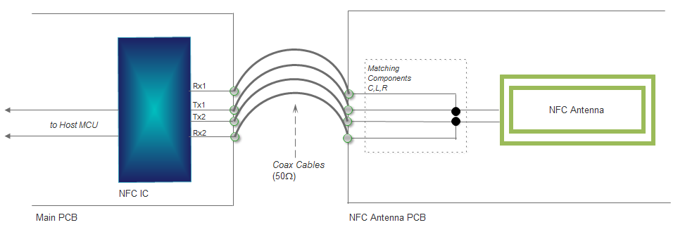
In our application we have to locate the NFC antenna (the inductor, actually) away of the PCB of the NFC IC 

The NFC antenna will be cast inside distanced PCB with connectors at the end of the antenna conductors. then we plan to run a "rail" to the distanced PCB of the NFC IC, MCU etc. and connect to the PCB connectors-->matching components-->NFC IC. 

Total distance between antenna and NFC IC 30-40cm. size of NFC antenna could be up to 10*5 cm or so. 

my Q's are-

1. possible? 

2. what would be the effective distance? 

3. if possible, which lines should I use as rail between antenna PCB and main PCB? 

attached sketch of the subject.

THX!

Ram

  • Hi Ram,

    It should be possible to do this.

    By rail, do you mean PCB traces? Usually a coax cable or something like that would be ideal for the antenna?

    Couple things to keep in mind, antenna tuning wise you will want to include the "rail"/coax in the tuning for the 50 ohm match point in order to prevent the parasitics from the cable from affecting the tuning, center frequency, bandwidth etc of your antenna.

    Another thing is to make sure that the long line isn't subject to noise/interfere which would corrupt the RF signals over that distance. What kind of environment will this be in?

    What did you mean by effective distance? I don't quite understand that question.
  • Hi Ralph,

    Thanks for your reply.

    Let me be more clear- the antenna PCB must be connected to the main PCB. both PCB's are distanced by ~40cm from each other. at the end of each board there will be connecters for the coax cables (as you wisely suggested). Now, when I wrote "effective distance" I meant what would the distance that will asure proper operation of the NFC.

    So, let me see if I understood it correctly-

    The antenna PCB will be cast as the size of the conductors, and its termination wou8ld be coax connectors.

    the rail (which mean, the cables that aren't PCB traces) will be connected to those connectors by means of coax cables that will be connected on the main PCB side to coax connectors.

    then, a 50ohm matching and filtering will have to be done before entering the NFC IC.

    BR,

    Ram

  • Hi Ram,

    Sorry for the delay in getting back to you. I checked over this with a hardware expert and yes your understanding is correct for the most part.

    One key thing to note is that the 50 ohm matching which is done before entering the NFC IC should be handled on the NFC Antenna side. So that Matching components C,L,R block you have diagrammed in your initial post would move from the Main PCB to the NFC Antenna PCB. This allows 50 ohm impedance to travel through the length of the coax cable for the ~40cm instead of the impedance of the antenna which is much lower, and this will provide a better signal to the NFC IC.

  • Hi Ralph,

    verified your answer, thanks for helping.

    attached the sketch for the final design-

  • Ram -
    with a TI based NFC/RFID system, you would only need the one 50 Ohm coax cable.