This thread has been locked.

If you have a related question, please click the "Ask a related question" button in the top right corner. The newly created question will be automatically linked to this question.

PCB width and layers' quantity.

Other Parts Discussed in Thread: CC2430, CC2591, CC2511, CC2420, CC2531, CC2530, CC2540

Hello.

I'd like to maximize the performance of my CC2430 design and therefore would like to follow exactly TI's design.

I already followed TI's reference design, related to components selection and schematic.

Now, I want to follow their PCB manufacturing, and therefore have a number of questions:

1. How many layers should the PCB have?

2. What should be the PCB's width (if it depends on the amount of layers - 2 or 4 - please specify the width for each).
(in the 'CC2430+CC2591 according to swra214' I saw that you recommend 1.6mm 4-layer PCB, but i read here that you recommend 1.2mm 2-layer PCB, so i'm confused).

3. How many oz. of copper should the PCB use?

If it helps to answer the question, i'm using a single ended antenna.

Thank you very much for any help.

  • The CC2430Em reference design is at http://focus.ti.com/general/docs/lit/getliterature.tsp?literatureNumber=swrr012c&fileType=zip

    . It has all of the information you are looking for. The following was taken for one of the read-me files.

    PCB DESCRIPTION:2 LAYER PCB 1.0 MM
      Dimensions in mil (0.001 inch)
                    DOUBLE SIDE SOLDER MASK,
                    DOUBLE SIDE SILKSCREEN,
                    8 MIL MIN TRACE WIDTH AND 8 MIL MIN ISOLATION.

  • Hi Stewart,

    CC2591EMK reference design read-me file writes:

    PCB DESCRIPTION:4 LAYER PCB 1.6 MM

    Copper 1 35 um

    Dielectric 1-2 0.35 mm (e.g. 2x Prepreg 7628 AT05 47% Resin)

    Copper 2 18 um

    Dielectric 2-3 0.76 mm (4 x 7628M 43% Resin)

    Copper 3 18 um

    Dielectric 3-4 0.35 mm (e.g. 2x Prepreg 7628 AT05 47% Resin)

    Copper 4 35 um

    DE104iML or equivalent substrate (Resin contents around 45%, which gives Er=4.42@2.4GHz, TanD=0.016)

    1. Does that mean that board is designed without a core, but only based on prepreg?

    2. Which dielectric/isolator is finally used: Prepreg 7628 AT05 47% Resin or DE104iML?

    3. What can one expect when used dielectric/isolator is replaced to:

    a. FR4

    b. Rogers RO4350


  • Hello

    The "core" is between layer 2 / 3, it is the same basic material as the pre-preg but purchased as sheet stock to have a solid material to build the layers up on. They are both similar to FR-4.

    If you were designing a narrow notch filter or resonant element for an oscillator with transmission lines the Er of the material would be very critical, but you are not.  The majority of the matching is done in lumped elements (Ls and Cs) which may benefit from the lower stray shunt capacitance resulting from a thicker substrate or the Rogers material with a lower Er (3.66).  A wave length in air at 2.4GHz is 12.5 cm, for microstrip it is scaled by 1/(sqrt Er) which is 6 cm for a Er of 4.3.  A 0.5cm transmission line is only 8% of a wavelength at 2.4GHz and 3% at 1GHz.  Whether the line is 50 or 65 ohms you will see little difference in the performance.

    The impedance of a transmission line is set by its Width over the dielectric thickness (Height).  That is from the top trace to the ground plane which is layer 2 on a 4 layer design. Note it does not matter how many additional layers there are or the total thickness of the board.

    When using a reference design it is important to maintain the W/H of the transmission line. If the W/H is 1.9 (for 50 ohms on FR4) on a 4 layer design with a .35mm layer 1 to 2 thickness and you switch to a single layer board that is 1.5mm thick the transmission line must get 1.5/.35 or 4.2 times wider. This is to maintain the W/H ratio and the designed impedance. Above I wrote the line impedance is fairly insensitive to small changes (+/- 15%) in width or the Er of the material.  A change of 4.2 times is not little and would impact performance in a bad way.

    At ½ ounce copper and up there is little impact of performance. As the material gets thicker the impedance will shift down very slightly. If you go thinner than ½ ounce copper its “skin depth” at 2.4GHz will exceed its thickness and will start to become lossy.

    The Rogers material is very similar to FR4 but with a slightly lower Er (3.66) and a little less loss. A W/H of 1.9 is 50 ohms on FR4 and is 53 ohms on 4350 due to this difference. With one T line of less than 10% of a wavelength you will never see the difference.

  • Stewart,

    Thank you for the clear answer,  very helpful.

    Cheers,

    Glasbergen

  •  

    Hi Glasbergen, I've had some successes with CC2430 PCBS. Let me offer a little experience.

    Impedance control is essential for good yield but don't try to second guess your PCB supplier on the properties of materials. You can take a first pass at the layout and call out nominal dimensions as a stating point.  In the end your PCB house will know more about dialing in their process to hit a specific impedance. Call out a specific impedance for your RF traces on the fab drawing like “20 mill trace with a 10 mill dielectric over the RF ground plane equals 50 Ohms +/- 10% at 2.4 GHz” and let the guys at the fab house do the fine tuning. Most fab houses are doing high-speed digital PCB these days and impedance testing with Time Domain Reflectometers is common. Ask for a test coupon and report on your array.

    The CC2430 reference design was, to put it nicely, and odd choice of dimensions: 40 mill dielectric thickness and 80 mill RF trace are uncommon, but that is what the stack-up works out to for 2.4 GHz. The PCB Balun is a conundrum.  I would go with the Anaren Balun and take a look at the CC2511 PCB for a more rational approach to 2.4 GHz layout. Any more questions send me an e-mail. 


  • Hi Stewart,

    It is my first time drawing a PCB board and I am completely lost. I downloaded the CC2430EM reference design. But I do not know how it can be useful. I use Altium Design 6.6. The CadStar_files.zip in the folder includes a .pcb file but there is no way to import it to altium designer. 

    Right now, I only understand PDF files in CC2430EM_PDF_RD.zip but they can not be imported to Altium Designer. I just got out of coding with CC2430 and started hardware design.

    Can you please explain the meaning and usefulness of files in these folders, like which are for reference only, which can be imported to Altium Designer? The folder TI provides should be of industry standard but I did not read any articles explaining how to start with such standard PCB information.

    Besides, I am not sure how to draw a transmission line in altium designer. How is transmission line different from a normal PCB line?

    Thank you very much.

  • Hello Arbi,


    This is Chris Pinter with Pinter Electronics Consulting.   I am an RF Engineer and while offer you some suggestions.  If you need to get a hold of me directly please visit   www.pinterec.ca


    To answer your questions:

    1.   Generally speaking a RF board can have as many layers as you need.  However the layer right under the components needs to be flooded with ground to eliminate noise and channel return current.  The TI evaluation boards are all two layer boards where the bottom board is flooded with a ground layer.  Note there are also many via holes to ground.  

    2.  The PCB width can be any width you like. However the transmission line width will need to be adjusted for impedance and routing depending on the width, or distance between layers.    The width of 1.6 mm 4 layer and 1.2 mm 2 layer is giving you two different options.  The key point to note here is the transmission line width is not defined.  That is the important missing information.

    3. The amount of copper you should use depends on the current that will go through the trace and the PCB fabrication process.  Generally speaking for RF designs I use 0.5 oz or 1 oz.

    Doing a layout for an RF circuit can be very complicated and if you need more help just give me a call.


    Hope this helps,

    Chris Pinter

    Senior RF Engineering consultant


  • I can try to help but there a lot of different subjects and disciplines involved assuming you are designing a custom board and not just trying to make more CC2430EMs.  We will need to work together to get this done.

    Altium Summer2009 has a tool to convert CADStar files, I have attached the converted files. They open in Altium 2009 and look good. See if you can open them in 6.6. The CAD Star library files were not available for conversion.

    When I started designing my first board (I’ve now done over 50 boards) I spent a lot of time in the fog of which tool, can I find library parts, which fab house etc. I have since learned that is just not that hard.  I suggest you capture the schematic in Altium first, get that right, I can go over it, and then worry about the PCB layout. PWB layout tools have a lot of features to make sure the layout matches the schematic provided they are linked.

    The numerous files provided by Ti can be used in a number of useful ways. I’ve seen one person actually make photo masks using the pdf images and use them to etch the circuits. For the most part they provide a “reference” design.  That is a design you refer to as you do your new design. Since most designs are unique, sometimes fitting in key Fobs, and other shapes, some have features like Li-Ion battery charges, CODECs, displays, buttons, etc.  The RF portion of the reference designs are more critical and must be replicated as close as possible.

    Transmission lines in Altium are just another trace on the PWB. What makes them a transmission line is they have a specific electrical length and impedance over a specific frequency band. Length is pretty clear; impedance is dependent on the width (w for width) of the line, the thickness (h for height) of the board material between the line and the first ground plane, and the dielectric properties (Er) of the board material. Sharp bends and other material placed too close to the line will affect its impedance. To a lesser extent the thickness of the line affects impedance. Assuming ½ to 1 oz copper the lines are thin enough that this effect is secondary.

    Impedance – A perfect line can be modeled as L’s and C’s. While it is expressed in ohms it is not a resistance. A line that is roughly  twice (w/h = 1.95) as wide as the dielectric is thick (e.g. 20 mils wide / 10 mils board thickness) on standard FR4 PWB material will have an impedance of  close to 50 ohms.  If  a length of such a line is connected to a 50 Ohm resistor and a wave sent down the line, all of the waves energy will be dissipated in the resistor and very little of it will be reflected back towards the signal generator.  Thus the line is said to have a characteristic impedance of 50 ohms.   This is rather long but the take away is if  the number of layers or other factors change the board thickness between the transmission line and the first ground plane the width of the line will have to change to maintain the line impedance.

    CC2430-CStoAltium.zip
  • Thank you very much.

    After reading cc2430 datasheet, I understand it a bit more. I downloaded a trial verison Altium Designer 09 Summer. It works. Now I know basics about antenna and balun.

  • Hi Stewart. I would like to ask a few more questions since you also use Altium 2009. I am using Altium Designer 2009 Summer. I converted both CC2430DB reference design and CC2430EM reference design to AD 2009 Summer. CC2430EM looks fine and makes sense but CC2430DB looks very messy. I attach screenshots of them here:

    CC2430DB:

    :

    CC2430EM:

    CC2430DB's PCB layout is messy as you can see above, but the schematics still make sense. So I use CC2430DB schematics as a reference for my customized design. After 1 day's of work, compilation is successful. However, the components converted from Cadstar do not correspond to any package in AD 2009 Summer (after I ran "Import Changes From xxxx.PrjPCB", in "Engineering change order",  I got a lot of RED cross marks with error message like "unknown pin: Pin xxx,xxx" which suggests components do not correspond to packages ). Did you replace those resistors, capacitors by components that can be found in AD 2009 manually?

    Also, I am not sure even if I can successfully convert schematics to a PCB, it will be different from the PCB layout provided in the reference design. So what I have to next is to tidy the PCB so that it looks almost identical to that in the reference design (at least in the antenna part)?

    TI suggests that we'd better follow reference designs as close as possible. Does it mean that after we obtained PCB from schematics, we replace the antenna and balun parts by that in the reference PCB design?

    Apologize for the long question. Thanks if you can take a look.

  • Hello,

    I imported CC2430DB into AD Summer09 Sp1 and got the same results as you. I used Tools/Component placer to expand the parts into something where I could at least see all of them. Obviously something is getting lost in the translation and while this layout might be optimized for minimum net length it is certainly NOT a suitable layout. The schematics opened nicely but as outlined below they are just “art”.

    If you would like I can “walk” you through the first PCB design. The first step is selecting the right tool. I think Altium is best out there but its $3995 (be sure they throw in a nanoboard) and a 30 day trial may be a bit short. One approach is request a longer period, like 6 months or more,  or use a free download (I like pcb123). Altium is a serious tool and a good skill to have.

    The Ti reference design files for CADStar do not include the library files thus the schematic files are basically just “art”. Step one is to go through and assign symbols from the AD library to the schematic and create the ones not available in the AD library and assign them to the symbols on the schematic. Now you can go through and assign footprints to the symbols on the schematic. Many are in the AD library, I can send you some and you will need to make a couple. They are easy with a little guidance. I see people hung up because a foot print or symbols is not available and I do not understand this. They are quick to make and every time I use one from a library I seem to have a problem with it.

    Notice everything so far is the schematic. The schematic in PCB design is King. The PCB layout tool will not let you make a connection different from the schematic, it is the source of foot prints and pin allocations. Once the schematic is complete you are 90% done.  All that would be left to do is set the layer stack up in Designs/Layer Stack Manager, assign the planes,  print the layer_1- CC2430DB_1_3.pdf file and place the parts as shown and connect them.

    Last the CC2430EM is a good starting place (you still need to complete the schematic with symbols and footprints). By adding a debug header, and a power connector you would have a complete unit and it would still be compatible with Ti Flash program, Packet Sniffer, and RF Studio which are all free down loads. You could add a header to access a few SPI and GPIO inputs, a couple of LEDs, a push button for further utility.

    Let me know how you want to proceed. My guess you can nail the CC2430EM schematic is a couple of days and have the tools to take on the DB design mostly on your own.


  • I really appreciate your generous help. Your explanation clears most of my doubts and I made a lot of progress today after reading your reply. After spending a whole day drawing the schematics as you suggested. The compilation is successful. I was able to create the netlist and went on to convert the netlist to PCB.  I did not start sorting the components in PCB yet. 

    And thanks for your kind offer to review my PCB. Hope you do not mind a few more questions. 

    1.  You suggested drawing PCB according to " layer_1- CC2430DB_1_3.pdf".  CC2430DB has 4 layers. Does it mean when I use PCB Board Wizard to initialize my PCB, I should select 2 power planes and 2 signal planes, and make the board parameters (like each layer's thickness, material used, etc) are exactly the same as CC2430DB? Can I choose 2 signal planes and 0 power planes (because I think 2 layer is cheaper and maybe later easier to debug)? 

    2. If I use 2 layers, that means I can not copy and paste from the reference design since substrate thickness affects microstrip's characteristic impedance. Am i right?

    3. In CC2430 schematics, there is a brown-out circuit in Power Source sub-schematic. CC2430 SOC has a built-in brownout circuit. So the brown-out circuit isn't necessary, is it?

    4. I am not sure if this is right. For crystal, capacitor values, I just put the value in Designator entry in Component Properties. The PCB fab house will know which component to put by looking at my schematics, right?

    5. Suppose I finished the PCB, I just send the PCB related files to the fab house. I requested a few free samples of CC2430 SOC chips. Should I give them to the fab house and tell them to solder on the right places? Can I also assume the fab house has crystals, capacitors, headers, pushbuttons, etc?

    Next, I will sort out the components in the PCB generated and copy the antenna and the balun parts to my PCB. I'll send it to you after completion. 

  • 1.)  2 versus 4 Layers    Your first consideration was cost. Using pcb123 V2 which gives instant quotes as you enter configurations a 1.5" X 1.5" board was $252 for qty 10   2 layer boards and $289 for qty 10   4 layer boards. $38 bucks or <$4 per board.  The biggest saving, over $150, is to not have a solder mask, but given 0402 size parts and QFN packages this is not practical. Once you have a solder mask having the designators silk screened onto the board is free. The advantage of 4 layers with power and ground planes is anywhere you need either power or ground you pop in a via and you are connected. Thru hole part and connectors VCC and GND pins are automatically connected These planes are continues sheets on copper with only a small clearance around other vias.  With ground on layer 2 you are guaranteed a continuous ground plane under everything on layer 1.

    The disadvantage of 2 layers is power is one more trace that must be routed point to point and you will find it  goes everywhere. Having all of these extra traces does not help trouble shooting.  It is mandatory you have a continuous ground without breaks from the start to the finish under of all RF lines. On simple boards using a copper pour connected to ground on both sides of the board this can be done. A quick look at the C2430EM is a good example. As complexity increases it approaches impossible fairly quickly.

    2.) Due to the need to route power and ground from pin to pin there is a lot of effort to port a 4 layer design onto 2 layers while maintaining a good continuous ground plane under the RF lines. It is not a simple cut and paste. Yes, the ratio of the width of the line (w) to the height ((h) thickness) of the board must be maintained for a given board material to maintain a certain impedance. The total thickness of the board does not matter, just h from the signal line to the ground directly under it.

    3.) I’ll have to look at the brown out circuitry tomorrow.

    4.) Designators are things like C4, R2, U1. In Altium if you click a schematic symbol and it shows green dots you can right click it and select properties. Here you can change the designator, enter the value (eg 10K, 1uF, 27pF), Red)  and many other things such as supplier data as well as assign a footprint. The value entered here shows on the schematic and parts list and can be used by the assembly house.  If you click on the designator and get gray squares and select properties you will see “Designator  -- Value”. It wants the “value” of the designator, like R2, it does not want 10K, this caught me the first time also.

    5. This is the question with the longest answer.  Here is a short version that leaves out a lot. This is for a small run of 2 to 10 boards. Large jobs (1000 boards) have far more options.
    a.) You well need to have a parts list that includes the manufactures part number for each part you use. You can add this info into Altium and it will print the list. I use Excel and can send an example. The Ti part list for the CC2430EM is a fair example.
    b.) Most often you order the board from a PCB fab shop and supply it to the assembly shop just like other parts. A few PCB fab shops are starting to offer small run assembly services.
    c.) Small run assembly houses are all different. They differ on how they want the parts supplied. Some will accept loose parts, some charge to tape your loose parts – other don’t, others will take short pieces of taped parts and others want full reels. Many will take a combination. That is they will accept your unique parts in loose (generally called bulk) packaging and will supply common parts such as bypass caps and resistors. Since they buy these common parts on full reels (up to 10,000 caps on a reel!) they get good prices and using reels they can use automatic pick and place machines. You need to design to their available parts inventory.
    d.) Many of the companies I work with on this forum have an assembler or two and build their own boards.

    It would be interesting to hear what shop other have found and how it is working for them.

    Personally I build all of my prototype boards using the following approach:
    a.) Order the PCB from a fab shop. Order the parts from digikey.com, mouser.com and others.
    b.) Order the solder stencil ($125) using the Altium Gerber file for the paste layer.
    c.)  Apply solder paste to the board using the stencil using a squeegee, using a microscope and a vacuum pick stick the parts in the solder paste. I then put it in a toaster oven until it reflows, the solder pulls all the parts into the right place, interesting to watch. Then I finish by hand soldering the thru hole parts. Then test. Figure 30 minutes for a board.  By the time you are set up to trouble shoot and rework a board to get it to work the first time you’re probably set to assembly it as well.

    After a few boards and the bugs are worked out I use a full service assembly shop supplying the unique parts on reels while using their common part also from reels. First run we’ll buy 100 to 500 boards.

  • Your reply helped me a lot in drawing my PCB. Thank you a lot. Now, I have my PCB drawing ready. I put it in my files area in this forum or you can access it from here  (http://e2e.ti.com/members/1186100/files/CC2430PCB.zip.aspx). It is based on CC2430DB and simpler than it. I deleted EEPROM, joystick, temperature sensors, etc and I replaced the original accelerometer by a more advanced accelerometer ADXL345 from Analog Devices. I used Altium Designer Summer Build 9.0.0.17654.

    Hope you don't mind a few more questions again.

    1) Regarding your answer for my question (4) , can the designators be any value? I mean R3 and R303 do not matter, but their corresponding values are important, right?

    2) Is manufacturer part list the same as BOM? In my BOM, the capacitors are grouped together under one row, which is different from the BOM for CC2430 which grouped capacitors by their values.

    3) Under the antenna of CC2430DB, there is no GND and VDD. I am not sure how to get rid of this area of power planes so what i did is placing the antenna out of the board area. Is is right?

    4) Should the polygon pour connected to GND or VDD or left unconnected?


    I am very much appreciated that you take the time to have a look at my PCB. :-) 


  • Hello  I'll open the pcb file later this morning. First the questions:

    1.) Designators:  Once again everything comes back to the schematic where the foot print and designator are associated with a symbol. When you go to layout the foot print and designator go together.  Designators are just labels and can be any number letter combination. You can use R1 but Rtherm, CAT or COW303 works to.

    2.) Here are a couple of lines from my parts list:

    You can see the manufactures part number, the supplier part number, designator, qty etc. It is a PBOM, Priced Bill of Materials. If you are not looking at the manufactures data sheet for the specific parts you plan to order and use, it is nearly certain what you will end up with parts that do not fit on the PCB or a PCB layout for a part no longer available in the package / footprint you grabbed out of a library.

    3.) You can not place parts out of the board area. PCB are made many on a sheet (called a panel)  of FR-4 or similar. After they are fabricated the sheet is cut into individual circuit boards. The "board area" determines where the panel is cut. What you want to do is delete the Plane1 (layer 2 which should be ground) in Stack up Manager and replace it with a Layer in Stack up Manager. Much like you draw the Polygon Pour on the top and bottom of the board you can add the Polygon Pour to this new layer. The important part is since you draw it you can decide what areas to leave un-filled.  A Plane is the same thing and it is nice because it automatically covers the whole area but is not the way to go when you want multiple planes or in your case an area without a plane.

    4.) The Polygon pour is typically connected to ground (GND) on the Top, Bottom, and Layer 2.


  • Hello

    I opened the file and overall it looks very good. Here are some comments; some of these may be the difference in how it opened in my configuration of Altium:

    Right click on MonitorSensor.PrjPCB in the left panel and add Existing files  MonitorSensor.SCHdoc and MonnitorSensor.PCBdocas well as the other schdoc files so they become sync'd and stay sync'd.

    In Stack up Manager the total board thickness is 1.3" or 34mm, could be a decimal point is missing on the middle layer.  The way you have it (core - prepreg-core) supports blind vias  but adds expense. It also does not provide as good of a ground plane or thermal performance.  Most quick turn board shops use a single board as a core and form the top and bottom layer with prepreg. I've used this with the CC2430 with good results.  As defined you have two cores separated by prepreg. It gives you better thickness consistency and is thicker, both help with the RF design and performance. In the pull down in Stack up Manager you can see the difference.  Key is to find out what your board house has and what it costs and then use those parameters.

    All vias should be set to go from top to bottom, not top to GND. This includes the ones under the devices. Right click via, properties and fix each one. There may be a global command but I have yet to find it.  The via attachs to the appropriate inter layers as they pass through. The GND vias shitch the top pour, inter ground layer, and bottom pour together causeing each to appear more continous.

    The bypass caps are too far away from the pins, same for the caps on the HF XTAL.  There could be a few more bypass caps. The wiring should be VDD via  - wire  - cap  - pin. Think of the bypass caps as a gate across the road, not off a side street some distance from the main road.

    Add a 100pF to .1uF cap from the /RST line (pin 10) to ground, leave off when first using Ti programmer. You will only need this when the device is fully programmed and ready for use away from the programmer. Without it noise will occasionally cause a reset.  Also the cap and R101 causes the /RST (not reset)  to rise slowly allowing the main power to approach full value before /RST become high enough to allow the device to operate. This prevents the device coming up in some funky state on occasion.

    You do not need the pull ups on the unused ports. They default to inputs with pull-ups after a reset (i.e. turn on). (Data sheet page 77 of 211) To be sure I include a few lines of code to do this as well.

    The board must extend under the antenna, replace the "Plane" with a "Layer" in stack up manager and then place a poly fill over the area not including the antenna. You may want to do the same for the layer 3 power plane. This will permit you to define a separate 1.8v and a 3.3v power plane if desired.

    I suggest adding another 2x5 header like P8 and route the SPI pins and maybe a couple of unused  I/O pins to it as a test port.  You may, or may not, have access to a logic analyzer today but if you continue with this type of project you will. There are several good ones for $150 to $390. The ability to "see" the 4 SPI in action and a GPIO port thrown in so you can see when a code point is passed really helps during development.  Even the abiltiy to hang a scope on it to see SCLK helps. It will save many hours of try this, try that.  Here are two I like  http://www.saleae.com/logic/ and http://www.pctestinstruments.com/


  • I adopted your suggestions to add another connector like P8. I have a saleae logic analyzer.

    Maybe your altium designer version differs from mine. Is the way to keep all files synchronized like this? I used this method.

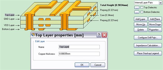
    I am not familiarize with PCB fabrication process. Do you suggest 'prepreg-core-prepreg' configuration? Please see the screenshot of my Layer Stack Manager.

    I selected the "Internal Layer Pairs" instead of "Layer Pairs".


    In PCB readme file of CC2430DB, it writes:

    4 LAYER PCB 1.112 MM NOMINAL THICKNESS WITH 0.35um Cu PER LAYER

    NOMINAL LAYER THICKNESS (NOT CRITICAL):

                    LAYER 1-2: 0.321 MM DIELECTRIC FR4 

                    LAYER  2-3: 0.34 MM DIELECTRIC FR4

                    LAYER 3-4: 0.321 MM DIELECTRIC FR4

                    Dielectric constant for FR4 is 4.5

    Thus, I defined copper thickness 0.00035mm (==0.35um),  made (prepreg=0.321mm, core 0.34mm, prepreg=0.321mm) and force Dielectric constant for FR4 to be 4.5. I am worried if the fabrication vendor can make FR4 with any dielectric constant. Also, I am worried that the copper thickness is too small, almost 1/100 of the default value. 


    I read some info about bypass capacitors and now know that they must be close to pins. But you said "There could be a few more bypass caps", do you mean adding a few more to battery and other power lines since bypass capacitors do not hurt anything and could only make things better?


    Thank you.

  • You seem to have mastered Altium.  Here is the glossary from Sunstone.com http://www.sunstone.com/customer-solutions/circuit-board-glossary.aspx  it is short but covers it all in detail with excellence guidance. I suggest you read it.

    I typically use Sunstone and like them but its where I had the first boards made using thier pcb123 v2 software and quick turn service and have not shopped around much so you may find one you like better.  I'm working with someone who uses PCBCART.com, his boards are blue with gold contacts and look great, he says the prices are great. The pcb fab house you choose will have a standard stack up that you will need to use.  Other's on this forum have correctly written you can specify the desired impedance and let the board house dial in the layer 1-2 thickness to nail it perfectly. This is true using a fab's full feature service and I have done this for a few customers but figure $1200-$1400 for a fab run instead of $330 using standard quick turn parameters.

    Bypass Caps:

    Notice the bypass cap placement is near the pin with a ground close to it.  The wire from VCC goes to the cap and then to the pin. With this arrangement the VCC line can be somewhat long. Pictured is a LNA/Power amp, like the RF section of the CC2430 placement is more critical here than on a voltage regulator or accelerometer. Space limitations do not always permit perfect placement. Sometimes VCC is routed directly to the pin with a short wire to the cap. In cases like the VR the cap is there to filter out ripple (<1 MHz) and will work when placed within inches of the device.  At times they are to low pass filter switching transients from logic drivers (<100MHz) and can be placed within ½ inch and near the line. The caps that are providing a RF ground at 2.4GHz and above need to be within 50 to 100 mils and should be wired directly to the pin. VCC should be applied at this low Z point to maximize the suppression of RF radiation. The ground point also must be placed close.  The  5 VDD pins (pins 27-31) are next to the RF pins and directly connected to the VDD_1.8 via with only one bypass cap 265mils away, the ground for the bypass cap is another 240mils away. One can check the box and say there is a bypass but in effect it is not doing much.  The reference design at http://focus.ti.com/general/docs/lit/getliterature.tsp?literatureNumber=swrr012c&fileType=zip has a variation for pins 27-31 in the Layer-1.pdf file that you lift directly.


    Hope this helps.  Once you get the next version set along the .pcbdoc and I'll take a look.

  • Hi, Steward :-) , I just finished the my 2nd drawing ( I was on leave in the past few weeks). I changed the wiring of bypass capacitors but a few like C231 and C241 are just too difficult to arrange. So I placed them just like that in CC2430DB. I hope that is all right. The whole file is in the folder under my account or you can access it here 
    Thank you very much for taking a look at my drawing.

  • Hello, 

    It is looking good. I have a couple comments for now, I'll look at it in more detail this evening.

    Flip pins 1 and 3 on X1 on the schematic to eliminate the need for the via in the line to X1. The xtal is electrically symmetrical so switching pins does not matter, having a via in the line may add noise or even prevent oscillation.

    There are many cases of the vias only going between two layers.  This is a necessary expense on high density boards but for this board I believe you would be better off if all of the TH and vias were "multilayer" start from top and going to bottom.  Two examples are pin 10 of P8, the pin continues to the bottom but has no pad on the bottom requiring a via to bring a line from the bottom to the top to attach to the pin.  The 2x4 ground via array at the top right has vias from the top to the GND plane. If the vias were top to bottom the bottom pour would also be connected to your advantage.  Blind vias add a process step to manufacturing the board that adds a lot of cost and precludes a quick turn around even if just one hole is blind. The layer 1-2 board must be drilled separately from the layer 3-4 board….

    For quicker service and lower cost the minimum hole size is 16mils.  8mils is the minimum for many shops but requires full service processing at higher cost and schedule.

    The power plane is split at the top of the board, I would suggest eliminating this portion of the plane altogether or eliminate the split.  Having a “free agent” dangling out there is an opportunity for some mischief, especially that close to the antenna.

    More later…


  • Hello foresightyj!

    I also got a lot of those, and it took me 2 days  to recogize th e problem (i don't have access to altium forum). I thougt that the libraries where not active / installed, but that was not it.

    In Project > Options > Comparator you have probaly marked Extra components as Ignore differences. This causes the the footpints to never get loaded when you update the PCB from schematics. mark it as find differences instead! That was the problem for me anyway.

    Tricky one : )

    //Olle,  Sweden.

  • foresightyj wrote...

    "

     I got a lot of RED cross marks with error message like "unknown pin: Pin xxx,xxx" which suggests components do not correspond to packages ). Did you replace those resistors, capacitors by components that can be found in AD 2009 manually?

    "

    Hello foresightyj!

    I also got a lot of those, and it took me 2 days  to recogize th e problem (i don't have access to altium forum). I thougt that the libraries where not active / installed, but that was not it.

    In Project > Options > Comparator you have probaly marked Extra components as Ignore differences. This causes the the footpints to never get loaded when you update the PCB from schematics. mark it as find differences instead! That was the problem for me anyway.

    Tricky one : )

    //Olle,  Sweden.

  • Thanks Olle. 

    I remembered that I did not solve the problem but instead I started my project from scratch and that problem never came out again. Now, under Comparator, they are all 'find differences'.


  • Hi Stewart,

    My latest work is here: http://e2e.ti.com/members/1186100/files/CC2430PCB-Second-Final-19_5F00_01_5F00_2010.zip.aspx

    Thanks for pointing out my buried vias. I forgot to update those beside the antenna. Now I changed to through hole ones. You mentioned pin 10 of P8. Are you just saying what I did is correct? I can't find anything wrong there.

    I added extra through hole GND vias on blank areas coz I think connection to GND will improve since it is more evenly distributed. I also widened a few wires as long as area allows.

    It is hard to get minimum via hole size of 16 mils. In particular, the via close to pin 21 of CC2430. I can't get it to 10 mils. Instead of cost, my worry is whether 8 mils is enough for handling the current of that pin.

    I've been in contact with a local PCB fab agent. I asked him a few questions. I just want to check if his answers are the same as what you did.

    1) He said his FR-4 has a dielectric constant varying from 4.2-4.7 which he has no control over.  He suggests that I could identify my transmission lines (for balun and impedance matching) and he could calculate and change the width of those parts for me. I drew the balun according to TI's documentations. Each line has precise length, width and position. If they change the width of them, is it going to affect the function of the balun?

    2) The vendor also provides assembly service. As for a few components which are also found in CC2430DB part list, like crystals X1 and X2, the brown out detection module EM6353, he said only if he had or he could find the components for me, otherwise I have to find them myself or change my design. Is it easy to find those components? or can I use other substitutes with similar specifications?


    Thanks :-)

  • The first photo show Pin 8 and 9 fed through a via. The second photo show the via deleted and the line connected directly to the header. I shelved the Polys for clarity.


     The long line from the array of GND vias in the 3rd photo needs a ground on the left end else it will couple to the antenna due to its length and proximity to the antenna.


    Question 1 /A1 You have done a great job of capturing the layout perfectly and notes for the reference design including the stack up. If your local shop can give you something close to  the .321mm (12.637mils) thickness for layers 1-2 it is the best you can do and it should work fine. (Note: Layer 2-3 and 3-4 thickness does not matter)

    Ti used Er=4.5 because it is in the middle of the range.  A shop can dial in Z (impedance) by adjusting the width of a line as written by others. This works for a Zx transmission line terminated with a Zx load.   Dial a line into 50 ohms with a 50 ohm load at the end and there will be no reflection, all of the power gets to the load. It does not matter how long the line is.   For the balun it's only half the story.

    Er (dielectric constant) is the velocity of the wave in the board material as compare with in the air. A wave travels at about 47% the speed of light in the micro-strip lines on FR-4 with a Er = 4.5. Why do you care? For this design the electrical length of the lines is as ( or more ) critical  as the impedance. The electrical length is a question of "how far does the wave travel in the time period of a cycle?" Since its speed is a function of Er, as Er varies the lay out length of the lines must change to be a certain electrical length as Er changes.  To adjust the length of the lines to accommodate a different Er  is a major task requiring a good  software tool like ANSOFT.  So, get the Layer 1-2 thickness close to .321mm as shown in the reference design and do not worry about Er being 4.2 - 4.7, you have "centered" the rest of the design on the reference design..


    Q2 / A2  The best places for parts are mouser.com and digikey.com. They have nearly everything, they take VISA, AMEX, MC etc, they ship the same day, and offer USPS Priority so you have your parts the 2nd day after you order them from Digikey and the 3rd day after from mouser.  


    I also get the standard parts list from my pcb assy house. They are good for bypass caps,  resistors, 0603 LEDs, headers and sometimes things like small SMT switches and USB connectors.  Be careful with the parts used in the balun and antenna circuit. They often do not have the high frequency parts like NPO caps and LQW15ANxxxxxx high Q inductors.  These you need to order and supply.

    Using  digikey and mouser I would identify available parts and get them on a parts list before I ordered the PCB, nothing worst than a board ready to build with a part that is 26 weeks lead time holding you up. Once you have the parts list have the local pcb shop tell you which one's they have and order the rest.


    The only part you may have trouble finding is the Brown Out device (M6353_1_8V), personally I would leave it off the board even if I had it, it does not do anything for me.

    Clean up: The board is in good shape and ready to order.  A trick you may know is to turn off the polys and set the pads and vias to draft.  This way you can see the top and bottom lines and how they meet under the pads and vias. All looks well except for some tails here and there and a via off P7 Pin 3 that does not go anywhere.


  • HI, Mr. Stewart,

    I completed the drawing. I placed a few more vias in the long strip in your 3rd screenshot above and cleaned up things under pads and vias. I guess I am set to go. I also started exploring mouser and digikey. 

    I know a bit about microstrip, characteristic impedance, etc. You told me layer 2-3 and 3-4 thickness does not matter. It makes sense in my drawing since layer 2 are poured with a large area of GND. However, I checked CC2430DB drawing, beneath balun, layer 2 is not poured with GND, so is layer 3 and until 4 we have a wide area of GND. The substrate height is not just 0.321mm.    Am I just worrying too much?

    Thank you for pointing out my flaws and mistakes. And I also thank you for your advices, encouragements and precious time taken to clear my doubts.


  • Good catch, the performance would have been very bad if you had left this unchanged.  You must maintain the W/H relationship for the RF lines where W is the width of the line and H is the height of the line above the ground plane.  H in this case is .321mm + .340mm+ .321mm or .982mm.    My guess Ti lifted the CC2430EM design off a 2 layer .032” board.  There are 3 pieces of good news.

    1.)     Since the dielectric is now nearly 3 time thicker the design is less sensitive to small variations in thickness

    2.)     The thickness is mostly driven by the core thickness as opposed to the prepreg, prepreg thickness is much more process dependent and variable.

    3.)     You only have to remove the Layer 2 and 3 plane under the RF circuit be ensure that the performance of the reference design is maintained. A 10 minute task

    In the attached jpg you can see the area I would use a polygon cut out to remove the layer 2 material. Layer 3 can be the same while eliminating it totally on the right and left side.  Keep in mind that every where you have a bypass cap between VCC and ground you are tying VCC to ground (for AC) thus improving VCC as a ground plane, this is a good thing.

    I have looked at the CC2430DB design,  Ti went further removing the inter planes under the entire CC2430 section. Once again my guess is they just lifted the two layer CC2430EM design changing only what they had to.  Leaving the layer 2-3 under this part of the circuit does not impact the RF design and provides better bypassing, improved thermal under the SOC, the smaller H in W/H results in lower impedance lines for VCC etc, and better grounding for the SOC. Also you would have to route longer VCC traces while possibly compromising bypass placement if you went back to 2 layers in this entire section.


    Every time I see this circuit I notice the 16 vias under the device. I use 5, 9 is probably a better number. I use dia 36, hole 20. The way it is, is fine if the pcb shop is OK.
    You must have set up a special DRC rule for these.


  • Hi Mr. Stewart,

    I removed polygon pours on the 2 inner layers under the balun.

    On Design Note DN003, at the end of page 3, it says "The impedance of the traces in the balun is affected by the distance between the traces on layer 1 and the ground plane beneath. Both CC2420 and CC2430 EM reference design uses a 1 mm thick two layer board with FR4 substrate." This suggests under the balun, the board thickness must be 1mm in total. I guess the minor difference between 0.982mm (CC2430DB) and 1mm (CC2430EM) does not matter, the same as what you said -- 'less sensitive to thickness'.

    I removed a few vias. Is it because those large vias take too much area and the polygon pours hardly have any presence amid the gaps?

    I uploaded my latest drawing to the folder under my account in case you'd like to have a glance. http://e2e.ti.com/members/1186100/files/CC2430PCB-Second-Final-21_5F00_01_5F00_2010.zip.aspx

    Thank you :-)


  • The Read Me note in the Ti CC2430DB file adds up to .98. There is a 2% disconnect I would not worry about.

    The vias under the SOC have 3 functions, DC ground, RF ground and Thermal. For DC you could use 1 via so it is off the table. For thermal its the cross section of the copper times the number of vias. Roughly cross section is Pi * Dia * copper thickness which is 1.4mil for 1 oz copper, its thinner in the vias so we'll call it 1 mil. 16 .016" dia vias have about the same cross section as 9 28mil vias (.8mils vs .79mils). The copper thickness will be thinner in the 16mil hole but give or take they are the same.  For RF the larger via has lower inductance, but there are fewer of them so this turns out nearly even again. The larger via can be drilled faster, it plates faster and will be more consistent in quality leading to better yields, this is the main pay back. I used 5 36mil vias (cross section ~.57mils+ since the plating is a little thicker) without problems but suggest 9 x 28mils is better.  I set a special rule for these vias with a 1mil annular (30 dia 28 hole) and no thermal relief. Since they are through a pad this is ok with the board shop. They basic define where the holes through the pad goes. This pad needs to be changed from top layer to multi layer if it isn’t so it will show up on the back side.

    I have not followed every wire but have looked at debug port wiring, reset pull up,  and other areas that sometimes cause problem. They all look good.

    Be sure to get the silk screen text off the pads and add a something like "Company Name  cc Jan 2010" to get a bit of copy protection and know what version it is a year from now on the Overlay layer in the open area right below the antenna, it will not change the performance... 


  • Ps  If you do change the via sizes on the pads... After right clicking on the via  / Properties you can click Simple instead of Full Stack at the top of the dialog box. This will give you 1 number to change that will apply to all layers affected.

    I added the 9 vias to the CC2430 foot print and changed the pad to multi layer and changed the rule to direct connect to eliminate the thermal relief just for this pad. The pad interfered with 2 traces, including the 1.8 VDD on the power plane, that had to be pushed slightly.

    and

  • Hi Mr. Stewart,

    I never knew there were so much knowledge just in GND pad of CC2430. I thought there more vias there, the more connected it was connected to the ground and the better the performance. You answer from the inductance point of view makes a lot of sense to me since RF always requires careful considerations.

    Even though I changed the pad 49 into multilayer as you suggested, I am still wondering why (if you do not mind elaborate). Both CC2430DB and CC2430EB have only top layer pad on pin 49 and thermal relief around the 9 vias on bottom layer. Top layer and multilayer pad on pin 49 both are equivalent to me except the multilayer pad is more connected to the GND.

    Anyway, I guess I nearly finished the drawing. Thank you very much for your great help.

    P.S. In case you want to have a glance, I uploaded my PCB here: http://e2e.ti.com/members/1186100/files/CC2430PCB-Second-Final-23_5F00_01_5F00_2010.zip.aspx

  • Hi, arbi tel,

    I am a green hand in the PCB area. Since I nearly completed one, I have some comments.

    1). 2 layer (like CC2430EM) and 4 layer (like CC2430DB) are both OK. Of course you will find in 4 layer, it is much easier in routing.

    What you need to make sure is the thickness between the balun & the antenna on top layer to the GND layer beneath them.

    In both CC2430EM and CC2430DB, the thickness is roughly 1mm. You can get this info from their Reference Design Read me files.

    2). PCB width makes sense only if we are talking about balun and antenna, there are design documents for how to draw them precise. I don't know why they should be that way though.

    I never read swra214 but I think you only have to make sure the thickness of the microstrip for those transmission line areas (antenna and balun) is what is specified in reference designs.

    The PCB board thickness is not important but the thickness in the sense of microstrip transmission lines. 


    3) I use 1 oz of copper (Actually I only realized and changed to 1 oz when replying to your questions). My design is based on CC2430DB. In CC2430DB Reference Design Read Me file,  it uses "4 LAYER PCB 1.0 MM NOMINAL THICKNESS WITH 0.35um Cu PER LAYER"

    0.35um= 0.014mil which is not a common thickness coz it = 0.01 oz of copper, a crazy number. Please see Mr. Stewart's reply here http://e2e.ti.com/support/low_power_rf/f/155/p/31147/108890.aspx#108890


    Hope it helps.

  • Turn off single Layer mode to better see the silk text over pads,  DRC shows 71 silk to silk violations including "CC2430 SOC"  text on solder pad.. See photo.

     Turn on rule checking for silk to silk (set 0), silk to pad (set 6mils), antennas( set 0), solder mask sliver(set 4mils). Set the Solder Mask Expansion rule to 2mils.

    The typically green Solder mask board coating  is great stuff, solder will not stick to it causing the solder to flow where the metal is even when the solder paste looks shorted before reflow. The solder mask in the layout is a window in the mask that prevents  the copper pad from getting cover with solder mask  coating.  Solder Mask Sliver is the thin area of solder mask material between Pads.  You currently have 4mil expansion, with 9mils between CC2430 pads this leave 1 mil slivers. You can see it in the photo. Due to errors in mask alignment etc this will end up with breaks in it permitting solder shorts that can not be cleared. Just change the expansion rules as above and all will be redrawn after you re-pour the polygons. 


    For future reference it is better to have a 8 mil expansion with less by rule for specific components that require it.  Key is to have the maximum sliver between parts to minimize solder bridging and 4 mils is the minimum to be effective.  Better to have solder mask covering a bit of copper pad that have shorts under a QFN or BGA. When you create a footprint think about the gap between pads and how much of it will be solder mask expansion and how much will be solder mask silver.

    The text has to be moved from the pads, next drawing the outline of the board with a line on the keep out layer, this is used by the fab house to set up the saw to cut the board from the panel, then you are ready for fab.  It would be good to change the expansion to 2mils for all or better is 2 for the CC2430 and ADXL345 by rules and set All to 8mils. The 1 anttenna DRC error is on the wide VDD line near C104 and can be ignored.  From transmission line theory open circuited stubs behave like shunt caps and are bad on high speed lines. On a DC line it does not matter.

    Next is the fun of creating the Gerber file folder which I find frustating in Altium. Under file you select Fabrication files select Gerber which creates a CAMcastic folder. In this folder you select Gerber again to actually create the Gerbers.  Select 2-3 for xx.xxx data format, make sure you do not include mechanical layers in the output. Last you need to view the Gerbers to make sure you got it right. Download ViewMate from http://www.pentalogix.com/ (it is free) and recomended by various fab shops.

  •  

    Hi, 

    I would never know the importance of these rules until you stated above. You made the reasons very clear to me. Thanks very much.

    I set up all the rules and cleared all violations. However, I found only about 63 violations. Not sure if it is due to version differences in Altium Designer.


    I tried ViewMate. However when opening my .GTL file, it gave me a self-intersecting polygon (SIP) error which I am not sure if you've ever encountered. The complete error message is ' ----WARNING----  Input contains a self-intersecting polygon at location (3.797 3.124) in layer 5. Do you want to auto-correct?'. I am uncertain if letting viewmate corrects it for me. Besides, I encountered some differences in displaying of the same .GTL file in Altium designer and viewmate. I got screenshots:


    In viewmate:


    In Altium Designer:

    Obviously, viewmate modified my gerber file. By the way, I am not sure about the purpose of trying gerber files in a gerber viewer. Is it to check compatibility of gerber files?


    Also, I have a doubt. When connecting crystals to CC2430, I widened some portion of the wires like net NetC191_2 below in XTAL X1, thinking wider wires may be better in passing current:

    However, when reading your comments on Net Antennae, in the junction of the thicker wire and the thiner wire, the high frequency clock signal may not flow fluently there. could it cause a problem?


    I have another question regarding calculation of load capacitors of XTAL X1. It is in my reply to another post http://e2e.ti.com/support/low_power_rf/f/155/p/15844/116925.aspx#116925 since someone else has a similar problem.  Could you please point out if I am doing it wrongly?

  • I forgot to mention the error with ViewMate. I ignore it and click no.  ViewMate is a quick check to see if the Gerbers look OK.  One time I had the "include Mechanical Layers" box checked which included a square box around all of the ICs on the top layer.  Every time I break my rule and import someone else's footprints I get a surprise; I've caught a few of these with ViewMate.  After all the board you get back is what is in the Gerber files you send out. I would not over analyze the ViewMate output, just watch for unwanted lines or text on a layer where it should not be suggesting a flaw in a foot print or an incorrect set up while exporting the Gerbers.

    I do not like the via in the XTAL path but Ti did it on the reference designs so it works.  The lines look fine. I’m more concerned about the lack of a ground near pin 2 of the XTAL. I would be inclined to push the XTAL to the right 60mils towards the edge of the board,  remove the ground via that is in the way. That would get pin 4 between two good grounds and open the space for a via near pin 2.

    I have used 15pf CPO caps for the XTALs without problem.  A reference design had suggested 22pF but the oscillator would not start at -10F. With the somewhat long and wide lines you have contributing additional shunt capacitance I would expect 15pF to be a good starting point.

    Overal the board and files look good.  It is time to get one fab’d.


  • Thanks Mr. Stewart. I understand your comments well except the load capacitors. Did you choose 15pF for both capacitors when you used NX3225DA which has a load capacitance of 16pF? Your answer seems to suggest that load capacitors do not have to be very accurate coz Ti recommended 33pF while you used 15pF. Or can I say as long as it is not far from 32MHz (for example, a few hundreds of ppm away) and oscillators run steadily, there will be no problem?

    15pF is a good starting point but it is not easy to do try-and-error on a PCB board. Forgive me if I am too concerned with accuracies since I have not much experience in this field and what I can master quickly is calculation. I selected another crystal which has a load capacitance of 10.6pF. Is it necessary to calculate exactly according to the formula given in CC2430 datasheet? And in case yes, what will be the best assumption for the value of C_parasitic?

    Thank you very much.

  • The NX3225SA-32.000M-EXS00A-02994 calls for a load cap of 16pF. I can not find  a NX3225DA.

    The xtal is tuned at the factory with a specific value of load cap. As you move away from this value (cap plus board capacitance)  the frequency will change from the specified value. In addition the SOC / xtal circuit needs a particular Q, real part, and noise else it will not start to oscillate. As you vary the capacitance you will find the point where it will not start before the frequency offset becomes a problem for the radio. The values that will work are fairly wide but the edges where it stops working are fairly sharp and change with temperature.  There is more tolerance on the high side so you are better off under estimating PCB contribution and therefore going with a little larger cap.

    Assuming a NX3225SA I would use two 12pF – 18pF C0G (often referred to as NPO) caps with a 1% or 2% tolerance. Both caps are the same and try to use the same manufacturer and part number on all of the boards that are to work together.

    For you circuit the parasitic capacitance is in the range of 2-3.5pF


  • Hi. Thanks very much and sorry to bother again. I still can not convince myself why you use two 12pF-18pF caps coz I think 33pF for both caps as recommended in CC2430 datasheet  is more reasonable since 33/2=16.5 which is roughly equal to load capacitance 16pF.

    Assuming using NX3225SA with load capacitance of 16pF, two C0G caps are 18pF and the underestimated parasitic capacitance is 2pF,  In the formula provided in CC2430 datasheet:

    C_load = (C191*C211)/(C191+C211)+C_parasitic

    the right hand side =18pF/2+2pF=11pF which is much smaller than the required 16pF.

  • …33pF is recommended….   Now exactly what part number crystal is that and what is its Cl?

    Per the Ti CC2430 data sheet, para 7.4 32 MHz Crystal Oscillator Table 8  Cl (C load) has a range of 10pF to 16pF with a typical of 12pF. (not written is this is dependent on the actual crystal selected) I started with 33pF per the reference design, found a few units that the oscillator would not start on a warm January morning in New Hampshire (--5F) and switched the caps out replacing them with 15pF (C0402C150J5GACTU) caps after doing the math, and have not had a problem since at any temperature up to +130F. 

    This is [(15x15)/(15+15)] + 2pF = 9.5pF After going to the manufactures web site for the specific crystal I was using and finding Cl to be 10pF I was comfortable with the selection of 15pF +/-5% NPO.  Since all of the units are about 40Hz above the crystal's design freq it indicates the Cl load value is close, and a little less than the specified 10pF which checks with the calculated 9.5pF. For one application we have a .5-2.5pF trimmer cap and dial all of the units in to +/- 5 Hz of the correct freq thus it help we have a Cl that is a bit undersized to start with.

    Step 1, check the manufacture's data sheet for Cl for the actual crystal you plan to order.


  •  

    Hi. Sorry that I may have confused you. The XTAL's part no is: NX3225SA 32MHz EXS00A-CS00189. It is probably a model only found in China coz I googled it and all pages are Chinese. The load capacitance is 10.6pF which falls in the range of 10-16pF.

    I understand how you ended up with 15pF now. Judging from your second last reply, I thought you were using NX3225SA-32.000M-EXS00A-02994 with a load capacitance of 16pF. Anyway, I think I'll go with 16pF initially coz 16/2+2=10pF and as you said I could underestimate C_parasitic by choosing larger capacitors.


    I am not sure how load capacitors affect XTAL's performance in different temperature environments. I am in Singapore and the temperature here is usually between 26-34 deg C. The operating temperature range of my XTAL is  -20 - +80 deg C. It is OK as long as the heat dissipation is not a problem.

    Thank you for helping me all the way.

  • Hi Stewart,

    What is the difference between Prepeg 7628 AT05 and 7628 AT01? I understand the resin content is different (47% vs. 45%) and they have slightly different Er . Will there be significant performance issues if  one uses AT01 instread of AT05 used in TI boards? Or as you mentioned,  as most of the matching is done in Lumped components slighly different Er will not be very critical.

    Thanks in advance!


  • Hello,

    Without seeing the actual design layout it is hard to say. The Ti reference designs and the typical layouts I have seen is not going to be sensitive to the slight difference between Er of the two materials. In those cases with printed antennas with transmission line matching the difference can shift the band a bit. For the last couple of designs I’ve completed I have removed the power and ground inter-planes in the area of the RF lines thus making the dielectric thickness that of the entire board.  This reduces the sensitivity to board thickness and Er making standard “quick turn” pcb processes more forgiving. The component pads have less shunt capacitance.   Also the T-lines are wider and therefore a very tiny bit less lossy.

    The biggest problem I see as I assist designers who contact me directly is their selection of chip caps and especially chip inductors.  Two different part number 0402 15nH inductors as measured at 100 to 200 MHz can be radically different when used at 2.4GHz. It is best to use the actual part numbers as used in the reference designs or a least compare and closely match their performance based on the graphs in the data sheets.


  • Hello, Arbi tel

    This is Alex, we are pcb and pcb assembly manufacturer from China. We have done pcb business nearly 20 years, and get a good reputation all over the world.

    If you are in need of PCB or PCB assembly, Please contact with me.

    Best regards
         Alex                       
    Wonderful PCB(H.K)Ltd                  
    Tel:+86 0755 86229518 ext.806

    Mobile: +86 15919925234
    Fax: +86 0755 26073529

    Skype: alexrain216
    ICQ#:561159768
    Email: wonderful04
    @wonderfulpcb.com
    Website: www.wonderfulpcb.com
                 http://wonderfulpcb.en.alibaba.com/
    Add: NanShan District,ShenZhen City, China

  • Hello,Stewart

    This is Alex, we are pcb and pcb assembly manufacturer from China. We have done pcb business nearly 20 years, and get a good reputation all over the world.

    If you are in need of PCB or PCB assembly, Please contact with me. I will quote you the price ASAP.

    Best regards
         Alex                       
    Wonderful PCB(H.K)Ltd                  
    Tel:+86 0755 86229518 ext.806

    Mobile: +86 15919925234
    Fax: +86 0755 26073529

    Skype: alexrain216
    ICQ#:561159768
    Email: wonderful04
    @wonderfulpcb.com
    Website: www.wonderfulpcb.com
                 http://wonderfulpcb.en.alibaba.com/
    Add: NanShan District,ShenZhen City, China

  • Hello

    This is Alex, we are pcb and pcb assembly manufacturer from China. We have done pcb business nearly 20 years, and get a good reputation all over the world.

    If you are in need of PCB or PCB assembly, Please contact with me. I will quote you the price ASAP.

    Best regards
         Alex                       
    Wonderful PCB(H.K)Ltd                  
    Tel:+86 0755 86229518 ext.806

    Mobile: +86 15919925234
    Fax: +86 0755 26073529

    Skype: alexrain216
    ICQ#:561159768
    Email: wonderful04
    @wonderfulpcb.com
    Website: www.wonderfulpcb.com
                 http://wonderfulpcb.en.alibaba.com/
    Add: NanShan District,ShenZhen City, China

  • Hello, Nobody

    This is Alex, we are pcb and pcb assembly manufacturer from China. We have done pcb business nearly 20 years, and get a good reputation all over the world.

    If you are in need of PCB or PCB assembly, Please contact with me.

    Best regards
         Alex                       
    Wonderful PCB(H.K)Ltd                  
    Tel:+86 0755 86229518 ext.806

    Mobile: +86 15919925234
    Fax: +86 0755 26073529

    Skype: alexrain216
    ICQ#:561159768
    Email: wonderful04
    @wonderfulpcb.com
    Website: www.wonderfulpcb.com
                 http://wonderfulpcb.en.alibaba.com/
    Add: NanShan District,ShenZhen City, China

  • Hi, Mr. Stewart.

    I would like to thank you for your help throughout my CC2430 PCB design. The PCB arrived a few days ago and it worked perfectly. Without your help, I couldn't be successful for the first time.

    Best wishes,

    Yuan Jian

  • I appreciate the feed back and I'm glad it work out well.

  • As the RF Engineer from TI who layouts the PCB boards I been following this Blog and most comments are correct.  In terms of this layout it was designed to reduce the cost of the balun/fileter matching network.  Therefoe the long traces which are part of the balun network.   

    The entire process of matching at high frequencies is to ensure the maximum power is delivered to the load.   You can use any one of three baluns to do this. 1) discrete components   2) intergrated solution  or 3) PCB strip line balun.     The trade offs are cost, size and preformance.    Baluns are used to take differential signals to single-ended and do the power match.   Most people focus upon the power match and don't pay attention to the baluns phase summing.  This takes two out phase signals and aligns them in phase so the total voltage doubles at the summing point.    The impedance match is done so to match a transmission line or antennas input impedance.  Often the balun output is not 50 ohms but lower value so the components values are larger for less variation in the circuit if discrete.   Another important point missed is the traces which are << than quarter wavelengths act as inductors.  Since the component values discrete steps are fairly large for these frequencies the traces are used to fine tune the phase by summing to the inductors in the balun.  Therefore the summing point has a (real + jzero) value.  The matching filter then is used to change the impedance to a transmission line characteristic impedance of 50 ohms.    Most layout designers don't like to pay for controller impedance lines so they use a line calculator and come up with the width of the line that is close and rely on the board vendors tolerance to maintain the 50 ohm line.   So if your product will have millions made then its safer to add another matching network between the antenna and the 50 ohm transmission line.    Also often the antenna is not exactly 50 ohms so including a matching network is good design procedure to follow.  You can always add zero ohm reistors if no matching is needed.

    Since board stackup is a way to size the width of the boards it also can be sued on multilayer boards to keep the same impedance.  By using the layer stacking and a good line calculator you can determine the reference designs line impedances and copy them to your prototype design.   Then use the component values from the reference design and you most likely will have maximum power to your antenna. 

    RRS

    TI Sr. RF Engineer

    Low Power Wireless & antennas

  • Hello,

     I have a similar problem as what is being discussed in this post. I am hoping to pose my question here and have the Guru's help me figure out the path forward.

    Using the CC2531 Donggle board as a starting point I removed the internal patch antenna that is specified on the Donggle reference design and copied the SMA antenna design from the CC2530-EM board reference design. In effect this means that I have married an antenna design specified for the 2 layer board to an 4 layer board. The track lengths and widths were unfortunately kept the same as specified in the 2 layer reference design. The thickness between the top layer and the first ground layer is 0.43 mm. The manufacturer states that the permittivity is 4.6 as opposed to the 4.5 specified by Ti in their reference design. I observe a loss of 14dB in receive power and 21 dB loss in transmit power as compared to the original TI reference design.

    Based on my calculation and posts by folks here, here is what I understand. The original TI reference design had a line width of 1.4 mm and a thickness of 0.8mm for the 50Ohm transmission line. This gives a perfect 50-Ohm transmission line. In my case this is now 33.5 Ohms. (since my w/h ratio of 3.24). 

    My questions:

    a) Should this change in 50-Ohm transmission line cause a 14 dB loss in receive power?  A simple simulation does not show that much difference. I am trying to figure out if there is some other problem in the PCB layout/design.

    b) The value of the inductance L252/L261 is specified as 2nH. L252/L261 is the inductances specified in the EM board reference design swrc144a. Even after using a 50 Ohm transmission line, in a simple RF simulation using rfsim99 I am not able to get a good S11 performance with 2nH. The circuit seems to work much better with 5nH. Can someone confirm the 2nH number?

    c) Is there any hope of using different matching components and regaining most of the loss in performance caused by a poor transmission line (34 Ohms?)

    Thank you, Sharat