This thread has been locked.

If you have a related question, please click the "Ask a related question" button in the top right corner. The newly created question will be automatically linked to this question.

RF430FRL152H: NFC communication(ISO 15693) + controlling port to GPIO(High/Low)

Part Number: RF430FRL152H

I have a question for using the chip rf430frl152h.

I want to read the voltage with an resistor using SD14(ADC) and transfer the conversion data usign nfc communication.

and also, I freely want to control P1.0/1.1/1.2/1.3 to GPIO(HIGH/LOW)

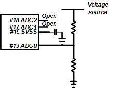
So, I am customizing the code as below based on the "RF430FRL152H_NFC_Only_Project"

P1SEL0 = 0xF0; //keep JTAG

P1SEL1 = 0xF0; //keep JTAG

P1DIR |= 0x0F;

P1OUT = 0x0F; // for making the P1.0/1.1/1.2/1.3 to output HIGH.

By the way, if the part "P1OUT = 0x0F;" is not in the code, nfc communication functions well.
But if the part "P1OUT = 0x0F;" is in the code, nfc communication does't do.

What do I have to do?

  • Hello Hyunwoo,

    I tried to check the phenomena you have described with my RF430FRL152EVM board. I have added the code as you did in the DeviceInit() but my NFC communication is still functional. I can not even see the reason why this setting ishould influence the NFC communication. Do you have anything connected to these port pins that maybe draws to much current out of the device?

    Best Regards,

    Helfried  

  • Thanks for your reply. But still, when I write that code, the programming is frozon in the middle by RF programming using TI.txt format file and GUI.
    Would you mind sharing your code?

    My code is below. I haven't modified any other part of code from the base code named "RF430FRL152H_NFC_Only_Project".

    void main()
    {
    WDTCTL = WDTPW + WDTHOLD; // Stop watchdog

    // ROM RF13M module setup ** The following three lines are needed for proper RF stack operation
    DS = 1; // ROM variable needs to be initialized here
    asm ( " CALL #0x5CDA "); // Call ROM function ( Initialize function pointers)
    asm ( " CALL #0x5CAC "); // Call ROM function ( Check part configuration)


    initISO15693(CLEAR_BLOCK_LOCKS);
    DeviceInit();
    SD14CTL0 = SD14EN + VIRTGND + SD14IE; //ADC enabled, Virtual Ground enabled, Interrupt enabled.
    SD14CTL1 = SD14UNI + SD14INTDLY0;

    while(1)
    {
    // Enter application code here...
    SD14CTL0 |= SD14SC;
    __bis_SR_register(LPM3_bits + GIE);
    }
    }

    void DeviceInit(void)
    {
    P1SEL0 = 0xF0; //keep JTAG
    P1SEL1 = 0xF0; //keep JTAG

    P1DIR |= 0x0F;

    P1OUT = 0x0F; 


    P1REN = 0;

    CCSCTL0 = CCSKEY; // Unlock CCS

    CCSCTL1 = 0; // do not half the clock speed
    CCSCTL4 = SELA_1 + SELM_0 + SELS_0; // Select VLO for ACLK and select HFCLK/DCO for MCLK, and SMCLK
    CCSCTL5 = DIVA_2 + DIVM_1 + DIVS_1; // Set the Dividers for ACLK (4), MCLK, and SMCLK to 1
    CCSCTL6 = XTOFF; // Turns of the crystal if it is not being used
    CCSCTL8 = ACLKREQEN + MCLKREQEN + SMCLKREQEN; //disable clocks if they are not being used

    CCSCTL0_H |= 0xFF; // Lock CCS

    return;
    }

    #pragma vector=SD_ADC_VECTOR
    interrupt void ADC (void)
    {
    switch(__even_in_range(SD14IV,4))
    {
    case SD14IV__NONE:
    {
    break;
    }
    case SD14IV__RES:
    {
    SD14CTL0 &= ~SD14IFG;
    ADC_Read = SD14MEM0;
    __bic_SR_register_on_exit(LPM4_bits);
    break;
    }
    case SD14IV__OV:
    {
    SD14CTL0 &= ~SD14OVIFG;
    break;
    }

    }
    }
  • Hello Hyunwoo,

    I will copy your code into my project to check that again, but I have limited time at the moment. I will come back to you the next days.

    Best Regards,

    Helfried

  • Hello Hyunwoo,

    I did an investigation of the problem you are facing. The problem with the port pin P1.0 and P1.1 you want to set is, that they are connected to level-shifters at the EVM board. When these level-shifters are not powered (1.5V missing) they start to draw current from the port pins. I have powered the 3.3V to generate the 1.5V with the regulator (IC1) to supply them and then it worked. Hope that helps.

    Best Regards,

    Helfried

  • Thank you for your reply. By the way, I have some questions. So, if I don't attach any other power source and regulator, can't I run gpio 1.0~1.3 with just rf power without connecting any other power? And In the code example for using adc and iso15693 communication, they have a declaration like below.
    PSEL0 = 0xF0 // keep jtag
    PSEL1 = 0xF0 // keep jtag 
    Is this necessary for using iso 15693 communication or adc?

    And can I use the gpio 1.4~1.7 to control pin?
    Like this?
    PSEL0 = 0x00 // keep jtag
    PSEL1 = 0x00 // keep jtag

    PDIR = 0xF0;

    P1OUT = 0xF0; 

    And I have a questions about rf programming.

    That the rf programming doesn't work has nothing to do with these things?
    So, for using rf programming properly, are there some regulations to be followed?

    In summary, in the code, those declarings
    PSEL0 = 0xF0 // keep jtag
    PSEL1 = 0xF0 // keep jtag 

    have something to do with iso15693 communication, using adc and rf programming?   

    Thank you so much for your answers in the meantime.
     

  • Hello Hyunwoo,

    you can use all the GPIO pins without connecting an additional power supply as long as you do not draw to much current from these pins. (i.e. trying to connect a LED).

    The GPIO pins P1.4 to P1.7 can be used as general IO pins or for the JTAG connection of an external debug probe. If you want to debug the code via JTAG you must keep the JTAG functionality. That is the reason why this code lines are added. If the JTAG functionality is not needed you can use these pins for own functions but for the price of the loss of the debug feature.

    Best Regards,

    Helfried 

  • Thank you for your answer. And I agree with your opinion.
    By the way, It seems I have found another possible cause of why my code is not working properly.
    When I first started this project, when I built the firmware code provided by TI, an warning did not occur.
    But I did update CCS version and compiler version in the middle, after that an warning continuously is occurred.
    #10325-D creating memory range $BOUND$0xf867 to accommodate BOUND.

    At present, when I built the raw CCS project downloaded from TI without adding and removing, that warning is occurred.
    Perhaps, Is the warning the reason that the code doesn't operate properly?
    If the answer is 'yes', how can I remove the warning? Should I have to change the compiler version? 

    I am really appreciated for your answer.


  • Can you please give me the version of the CCS and the compiler you are using? I haven't seen this warning before and have no idea why this is generated.

    Regards,

    Helfried

  • I am using the CCS with 10.2.0 and I tried to compile with every compiler is available. But every compiler showed the warning and additional warnings and errors are represented depending on compiler. Below is the compilers available.

  • I have checked that now with the same CCS version but do not get this warning. There must be something else wrong with your setup. Can you please send me your .map file that is generated when you compile your project. Maybe that can help me to find the reason for this warning.

  • Here is my .map file
    ******************************************************************************
    MSP430 Linker PC v4.3.8
    ******************************************************************************
    >> Linked Tue Apr 27 19:31:18 2021

    OUTPUT FILE NAME: <RF430FRL152H_NFC_Only_Project.out>
    ENTRY POINT SYMBOL: "_c_int00" address: 0000fe7e


    MEMORY CONFIGURATION

    name origin length used unused attr fill
    ---------------------- -------- --------- -------- -------- ---- --------
    SFR 00000000 00000010 00000000 00000010 RWIX
    PERIPHERALS_8BIT 00000010 000000f0 00000000 000000f0 RWIX
    PERIPHERALS_16BIT 00000100 00000100 00000000 00000100 RWIX
    RAM 00001c00 00001000 00000113 00000eed RWIX
    RF13M_ROM_ISR 000054d0 00000002 00000000 00000002 RWIX
    $BOUND$0xf867 0000f867 00000001 00000001 00000000 R IX
    FRAM 0000f868 00000468 00000015 00000453 RWIX
    FRAM_CODE 0000fcd0 00000300 0000023c 000000c4 RWIX
    JTAGSIGNATURE 0000ffd0 00000004 00000004 00000000 RWIX ffff
    BSLSIGNATURE 0000ffd4 00000004 00000004 00000000 RWIX ffff
    INT00 0000ffe0 00000002 00000000 00000002 RWIX
    INT01 0000ffe2 00000002 00000000 00000002 RWIX
    INT02 0000ffe4 00000002 00000000 00000002 RWIX
    INT03 0000ffe6 00000002 00000000 00000002 RWIX
    INT04 0000ffe8 00000002 00000000 00000002 RWIX
    INT05 0000ffea 00000002 00000002 00000000 RWIX
    INT06 0000ffec 00000002 00000002 00000000 RWIX
    INT07 0000ffee 00000002 00000002 00000000 RWIX
    INT08 0000fff0 00000002 00000002 00000000 RWIX
    INT09 0000fff2 00000002 00000002 00000000 RWIX
    INT10 0000fff4 00000002 00000002 00000000 RWIX
    INT11 0000fff6 00000002 00000002 00000000 RWIX
    INT12 0000fff8 00000002 00000002 00000000 RWIX
    INT13 0000fffa 00000002 00000002 00000000 RWIX
    INT14 0000fffc 00000002 00000002 00000000 RWIX
    RESET 0000fffe 00000002 00000002 00000000 RWIX


    SECTION ALLOCATION MAP

    output attributes/
    section page origin length input sections
    -------- ---- ---------- ---------- ----------------
    .TI.bound:DS
    * 0 00001c00 00000001 UNINITIALIZED
    00001c00 00000001 main.obj (.TI.bound:DS)

    .data 0 00001c02 00000008 UNINITIALIZED
    00001c02 00000004 rts430_eabi.lib : _lock.obj (.data)
    00001c06 00000004 : exit_gvars.obj (.data)

    .TI.bound:PF
    * 0 00001c0a 00000060 UNINITIALIZED
    00001c0a 00000060 main.obj (.TI.bound:PF)

    .TI.bound:RF
    * 0 00001c6a 00000001 UNINITIALIZED
    00001c6a 00000001 main.obj (.TI.bound:RF)

    .TI.bound:NRX
    * 0 00001ca4 00000022 UNINITIALIZED
    00001ca4 00000022 main.obj (.TI.bound:NRX)

    .TI.bound:NTX
    * 0 00001cc6 00000022 UNINITIALIZED
    00001cc6 00000022 main.obj (.TI.bound:NTX)

    .TI.bound:EL
    * 0 00001cf2 00000001 UNINITIALIZED
    00001cf2 00000001 main.obj (.TI.bound:EL)

    .stack 0 00002b9c 00000064 UNINITIALIZED
    00002b9c 00000002 rts430_eabi.lib : boot.obj (.stack)
    00002b9e 00000062 --HOLE--

    .rf13m_rom_isr
    * 0 000054d0 00000002 DSECT
    000054d0 00000002 main.obj (.rf13m_rom_isr:RF13M_ISR)

    .TI.bound:Firmware_System_Control_Byte
    * 0 0000f867 00000001
    0000f867 00000001 main.obj (.TI.bound:Firmware_System_Control_Byte)

    .TI.bound:NFC_NDEF_Message
    * 0 0000f868 00000015
    0000f868 00000015 main.obj (.TI.bound:NFC_NDEF_Message)

    .TI.persistent
    * 0 0000fcd0 00000000 UNINITIALIZED

    .cio 0 0000fcd0 00000000 UNINITIALIZED

    .sysmem 0 0000fcd0 00000000 UNINITIALIZED

    .cinit 0 0000fcd0 00000046
    0000fcd0 0000000c (.cinit..data.load) [load image]
    0000fcdc 00000006 (__TI_handler_table)
    0000fce2 00000004 (.cinit..TI.bound:DS.load) [load image, compression = zero_init]
    0000fce6 00000004 (.cinit..TI.bound:EL.load) [load image, compression = zero_init]
    0000fcea 00000004 (.cinit..TI.bound:NRX.load) [load image, compression = zero_init]
    0000fcee 00000004 (.cinit..TI.bound:NTX.load) [load image, compression = zero_init]
    0000fcf2 00000004 (.cinit..TI.bound:PF.load) [load image, compression = zero_init]
    0000fcf6 00000004 (.cinit..TI.bound:RF.load) [load image, compression = zero_init]
    0000fcfa 0000001c (__TI_cinit_table)

    .pinit 0 0000fd16 00000000 UNINITIALIZED

    .init_array
    * 0 0000fd16 00000000 UNINITIALIZED

    .mspabi.exidx
    * 0 0000fd16 00000000 UNINITIALIZED

    .mspabi.extab
    * 0 0000fd16 00000000 UNINITIALIZED

    .const 0 0000fd16 00000000 UNINITIALIZED

    .text 0 0000fd16 000001f6
    0000fd16 0000005e rts430_eabi.lib : copy_decompress_rle.obj (.text:__TI_decompress_rle_core)
    0000fd74 0000005e : autoinit.obj (.text:_auto_init)
    0000fdd2 0000003c main.obj (.text:DeviceInit)
    0000fe0e 0000002a rts430_eabi.lib : exit.obj (.text:exit)
    0000fe38 00000024 main.obj (.text:main)
    0000fe5c 00000022 main.obj (.text:initISO15693)
    0000fe7e 0000001c rts430_eabi.lib : boot.obj (.text:_c_int00_noargs)
    0000fe9a 00000014 : copy_zero_init.obj (.text:decompress:ZI:__TI_zero_init)
    0000feae 00000014 : memset.obj (.text:memset)
    0000fec2 00000012 : copy_decompress_none.obj (.text:decompress:none:__TI_decompress_none)
    0000fed4 00000012 : memcpy.obj (.text:memcpy)
    0000fee6 00000010 : epilog.obj (.text)
    0000fef6 00000006 : isr_trap.obj (.text:_isr:__TI_ISR_TRAP)
    0000fefc 00000006 : copy_decompress_rle.obj (.text:decompress:rle24:__TI_decompress_rle24)
    0000ff02 00000004 : pre_init.obj (.text:_system_pre_init)
    0000ff06 00000004 : exit.obj (.text:abort)
    0000ff0a 00000002 : _lock.obj (.text:_nop)

    $fill000 0 0000ffd0 00000004
    0000ffd0 00000004 --HOLE-- [fill = ffff]

    $fill001 0 0000ffd4 00000004
    0000ffd4 00000004 --HOLE-- [fill = ffff]

    RFPMM 0 0000ffea 00000002
    0000ffea 00000002 rts430_eabi.lib : int05.obj (.int05)

    PORT1 0 0000ffec 00000002
    0000ffec 00000002 rts430_eabi.lib : int06.obj (.int06)

    SD_ADC 0 0000ffee 00000002
    0000ffee 00000002 rts430_eabi.lib : int07.obj (.int07)

    USCI_B0 0 0000fff0 00000002
    0000fff0 00000002 rts430_eabi.lib : int08.obj (.int08)

    ISO 0 0000fff2 00000002
    0000fff2 00000002 main.obj (.int09)

    WDT 0 0000fff4 00000002
    0000fff4 00000002 rts430_eabi.lib : int10.obj (.int10)

    TIMER0_A1
    * 0 0000fff6 00000002
    0000fff6 00000002 rts430_eabi.lib : int11.obj (.int11)

    TIMER0_A0
    * 0 0000fff8 00000002
    0000fff8 00000002 rts430_eabi.lib : int12.obj (.int12)

    UNMI 0 0000fffa 00000002
    0000fffa 00000002 rts430_eabi.lib : int13.obj (.int13)

    SYSNMI 0 0000fffc 00000002
    0000fffc 00000002 rts430_eabi.lib : int14.obj (.int14)

    .reset 0 0000fffe 00000002
    0000fffe 00000002 rts430_eabi.lib : boot.obj (.reset)


    LINKER GENERATED COPY TABLES

    __TI_cinit_table @ 0000fcfa records: 7, size/record: 4, table size: 28
    .data: load addr=0000fcd0, load size=0000000c bytes, run addr=00001c02, run size=00000008 bytes, compression=copy
    .TI.bound:DS: load addr=0000fce2, load size=00000004 bytes, run addr=00001c00, run size=00000001 bytes, compression=zero_init
    .TI.bound:EL: load addr=0000fce6, load size=00000004 bytes, run addr=00001cf2, run size=00000001 bytes, compression=zero_init
    .TI.bound:NRX: load addr=0000fcea, load size=00000004 bytes, run addr=00001ca4, run size=00000022 bytes, compression=zero_init
    .TI.bound:NTX: load addr=0000fcee, load size=00000004 bytes, run addr=00001cc6, run size=00000022 bytes, compression=zero_init
    .TI.bound:PF: load addr=0000fcf2, load size=00000004 bytes, run addr=00001c0a, run size=00000060 bytes, compression=zero_init
    .TI.bound:RF: load addr=0000fcf6, load size=00000004 bytes, run addr=00001c6a, run size=00000001 bytes, compression=zero_init


    LINKER GENERATED HANDLER TABLE

    __TI_handler_table @ 0000fcdc records: 3, size/record: 2, table size: 6
    index: 0, handler: __TI_decompress_rle24
    index: 1, handler: __TI_decompress_none
    index: 2, handler: __TI_zero_init


    GLOBAL SYMBOLS: SORTED ALPHABETICALLY BY Name

    address name
    -------- ----
    0000ff06 C$$EXIT
    00000160 CCSCTL0
    00000161 CCSCTL0_H
    00000160 CCSCTL0_L
    00000162 CCSCTL1
    00000163 CCSCTL1_H
    00000162 CCSCTL1_L
    00000164 CCSCTL2
    00000165 CCSCTL2_H
    00000164 CCSCTL2_L
    00000168 CCSCTL4
    00000169 CCSCTL4_H
    00000168 CCSCTL4_L
    0000016a CCSCTL5
    0000016b CCSCTL5_H
    0000016a CCSCTL5_L
    0000016c CCSCTL6
    0000016d CCSCTL6_H
    0000016c CCSCTL6_L
    0000016e CCSCTL7
    0000016f CCSCTL7_H
    0000016e CCSCTL7_L
    00000170 CCSCTL8
    00000171 CCSCTL8_H
    00000170 CCSCTL8_L
    00000150 CRCDI
    00000152 CRCDIRB
    00000153 CRCDIRB_H
    00000152 CRCDIRB_L
    00000151 CRCDI_H
    00000150 CRCDI_L
    00000154 CRCINIRES
    00000155 CRCINIRES_H
    00000154 CRCINIRES_L
    00000156 CRCRESR
    00000157 CRCRESR_H
    00000156 CRCRESR_L
    00001c00 DS
    0000fdd2 DeviceInit
    00001cf2 EL
    0000f867 Firmware_System_Control_Byte
    0000f868 NFC_NDEF_Message
    00001ca4 NRX
    00001cc6 NTX
    0000020e P1IV
    0000021e P2IV
    00000204 PADIR
    00000205 PADIR_H
    00000204 PADIR_L
    00000208 PADS
    00000209 PADS_H
    00000208 PADS_L
    0000021a PAIE
    00000218 PAIES
    00000219 PAIES_H
    00000218 PAIES_L
    0000021b PAIE_H
    0000021a PAIE_L
    0000021c PAIFG
    0000021d PAIFG_H
    0000021c PAIFG_L
    00000200 PAIN
    00000201 PAIN_H
    00000200 PAIN_L
    00000202 PAOUT
    00000203 PAOUT_H
    00000202 PAOUT_L
    00000206 PAREN
    00000207 PAREN_H
    00000206 PAREN_L
    0000020a PASEL0
    0000020b PASEL0_H
    0000020a PASEL0_L
    0000020c PASEL1
    0000020d PASEL1_H
    0000020c PASEL1_L
    00001c0a PF
    00001c6a RF
    0000080a RF13MCRC
    0000080b RF13MCRC_H
    0000080a RF13MCRC_L
    00000800 RF13MCTL
    00000801 RF13MCTL_H
    00000800 RF13MCTL_L
    0000080c RF13MFIFOFL
    0000080d RF13MFIFOFL_H
    0000080c RF13MFIFOFL_L
    00000802 RF13MINT
    00000803 RF13MINT_H
    00000802 RF13MINT_L
    00000804 RF13MIV
    00000805 RF13MIV_H
    00000804 RF13MIV_L
    00000820 RF13MRXBUF
    00000821 RF13MRXBUF_H
    00000820 RF13MRXBUF_L
    00000806 RF13MRXF
    00000807 RF13MRXF_H
    00000806 RF13MRXF_L
    00000840 RF13MTXBUF
    00000841 RF13MTXBUF_H
    00000840 RF13MTXBUF_L
    00000808 RF13MTXF
    00000809 RF13MTXF_H
    00000808 RF13MTXF_L
    0000080e RF13MWMCFG
    0000080f RF13MWMCFG_H
    0000080e RF13MWMCFG_L
    000054d0 RF13M_ISR
    00000124 RFMMIE
    00000125 RFMMIE_H
    00000124 RFMMIE_L
    00000120 RFPMMCTL0
    00000121 RFPMMCTL0_H
    00000120 RFPMMCTL0_L
    00000122 RFPMMCTL1
    00000123 RFPMMCTL1_H
    00000122 RFPMMCTL1_L
    00000126 RFPMMIFG
    00000127 RFPMMIFG_H
    00000126 RFPMMIFG_L
    00000128 RFPMMIV
    00000129 RFPMMIV_H
    00000128 RFPMMIV_L
    00000700 SD14CTL0
    00000701 SD14CTL0_H
    00000700 SD14CTL0_L
    00000702 SD14CTL1
    00000703 SD14CTL1_H
    00000702 SD14CTL1_L
    0000070c SD14IV
    0000070d SD14IV_H
    0000070c SD14IV_L
    00000704 SD14MEM0
    00000705 SD14MEM0_H
    00000704 SD14MEM0_L
    00000706 SD14MEM1
    00000707 SD14MEM1_H
    00000706 SD14MEM1_L
    00000708 SD14MEM2
    00000709 SD14MEM2_H
    00000708 SD14MEM2_L
    0000070a SD14MEM3
    0000070b SD14MEM3_H
    0000070a SD14MEM3_L
    00000100 SFRIE1
    00000101 SFRIE1_H
    00000100 SFRIE1_L
    00000102 SFRIFG1
    00000103 SFRIFG1_H
    00000102 SFRIFG1_L
    00000104 SFRRPCR
    00000105 SFRRPCR_H
    00000104 SFRRPCR_L
    00000198 SYSBERRIV
    00000199 SYSBERRIV_H
    00000198 SYSBERRIV_L
    00000190 SYSCNF
    00000191 SYSCNF_H
    00000190 SYSCNF_L
    00000180 SYSCTL
    00000181 SYSCTL_H
    00000180 SYSCTL_L
    00000186 SYSJMBC
    00000187 SYSJMBC_H
    00000186 SYSJMBC_L
    00000188 SYSJMBI0
    00000189 SYSJMBI0_H
    00000188 SYSJMBI0_L
    0000018a SYSJMBI1
    0000018b SYSJMBI1_H
    0000018a SYSJMBI1_L
    0000018c SYSJMBO0
    0000018d SYSJMBO0_H
    0000018c SYSJMBO0_L
    0000018e SYSJMBO1
    0000018f SYSJMBO1_H
    0000018e SYSJMBO1_L
    0000019e SYSRSTIV
    0000019f SYSRSTIV_H
    0000019e SYSRSTIV_L
    0000019c SYSSNIV
    0000019d SYSSNIV_H
    0000019c SYSSNIV_L
    0000019a SYSUNIV
    0000019b SYSUNIV_H
    0000019a SYSUNIV_L
    00000352 TA0CCR0
    00000354 TA0CCR1
    00000356 TA0CCR2
    00000342 TA0CCTL0
    00000344 TA0CCTL1
    00000346 TA0CCTL2
    00000340 TA0CTL
    00000360 TA0EX0
    0000036e TA0IV
    00000350 TA0R
    0000065e UCB0ADDMASK
    0000065f UCB0ADDMASK_H
    0000065e UCB0ADDMASK_L
    0000065c UCB0ADDRX
    0000065d UCB0ADDRX_H
    0000065c UCB0ADDRX_L
    00000646 UCB0BRW
    00000647 UCB0BRW_H
    00000646 UCB0BRW_L
    00000640 UCB0CTLW0
    00000641 UCB0CTLW0_H
    00000640 UCB0CTLW0_L
    00000642 UCB0CTLW1
    00000643 UCB0CTLW1_H
    00000642 UCB0CTLW1_L
    00000654 UCB0I2COA0
    00000655 UCB0I2COA0_H
    00000654 UCB0I2COA0_L
    00000656 UCB0I2COA1
    00000657 UCB0I2COA1_H
    00000656 UCB0I2COA1_L
    00000658 UCB0I2COA2
    00000659 UCB0I2COA2_H
    00000658 UCB0I2COA2_L
    0000065a UCB0I2COA3
    0000065b UCB0I2COA3_H
    0000065a UCB0I2COA3_L
    00000660 UCB0I2CSA
    00000661 UCB0I2CSA_H
    00000660 UCB0I2CSA_L
    0000066a UCB0IE
    0000066b UCB0IE_H
    0000066a UCB0IE_L
    0000066c UCB0IFG
    0000066d UCB0IFG_H
    0000066c UCB0IFG_L
    0000066e UCB0IV
    0000064c UCB0RXBUF
    0000064d UCB0RXBUF_H
    0000064c UCB0RXBUF_L
    00000648 UCB0STATW
    00000649 UCB0STATW_H
    00000648 UCB0STATW_L
    0000064a UCB0TBCNT
    0000064b UCB0TBCNT_H
    0000064a UCB0TBCNT_L
    0000064e UCB0TXBUF
    0000064f UCB0TXBUF_H
    0000064e UCB0TXBUF_L
    0000015c WDTCTL
    0000015d WDTCTL_H
    0000015c WDTCTL_L
    00002c00 __STACK_END
    00000064 __STACK_SIZE
    0000fcfa __TI_CINIT_Base
    0000fd16 __TI_CINIT_Limit
    0000fcdc __TI_Handler_Table_Base
    0000fce2 __TI_Handler_Table_Limit
    UNDEFED __TI_INITARRAY_Base
    UNDEFED __TI_INITARRAY_Limit
    0000fef6 __TI_ISR_TRAP
    00000001 __TI_args_main
    00001c06 __TI_cleanup_ptr
    0000fec2 __TI_decompress_none
    0000fefc __TI_decompress_rle24
    00001c08 __TI_dtors_ptr
    00000001 __TI_exit
    0000ffea __TI_int05
    0000ffec __TI_int06
    0000ffee __TI_int07
    0000fff0 __TI_int08
    0000fff2 __TI_int09
    0000fff4 __TI_int10
    0000fff6 __TI_int11
    0000fff8 __TI_int12
    0000fffa __TI_int13
    0000fffc __TI_int14
    0000fe9a __TI_zero_init
    ffffffff __binit__
    ffffffff __c_args__
    0000fef2 __mspabi_func_epilog_1
    0000fef0 __mspabi_func_epilog_2
    0000feee __mspabi_func_epilog_3
    0000feec __mspabi_func_epilog_4
    0000feea __mspabi_func_epilog_5
    0000fee8 __mspabi_func_epilog_6
    0000fee6 __mspabi_func_epilog_7
    0000fd74 _auto_init
    0000fe7e _c_int00
    0000fe7e _c_int00_noargs
    00001c02 _lock
    0000ff0a _nop
    0000fffe _reset_vector
    00002b9c _stack
    0000ff02 _system_pre_init
    00001c04 _unlock
    0000ff06 abort
    ffffffff binit
    0000fe0e exit
    0000fe5c initISO15693
    0000fe38 main
    0000fed4 memcpy
    0000feae memset


    GLOBAL SYMBOLS: SORTED BY Symbol Address

    address name
    -------- ----
    00000001 __TI_args_main
    00000001 __TI_exit
    00000064 __STACK_SIZE
    00000100 SFRIE1
    00000100 SFRIE1_L
    00000101 SFRIE1_H
    00000102 SFRIFG1
    00000102 SFRIFG1_L
    00000103 SFRIFG1_H
    00000104 SFRRPCR
    00000104 SFRRPCR_L
    00000105 SFRRPCR_H
    00000120 RFPMMCTL0
    00000120 RFPMMCTL0_L
    00000121 RFPMMCTL0_H
    00000122 RFPMMCTL1
    00000122 RFPMMCTL1_L
    00000123 RFPMMCTL1_H
    00000124 RFMMIE
    00000124 RFMMIE_L
    00000125 RFMMIE_H
    00000126 RFPMMIFG
    00000126 RFPMMIFG_L
    00000127 RFPMMIFG_H
    00000128 RFPMMIV
    00000128 RFPMMIV_L
    00000129 RFPMMIV_H
    00000150 CRCDI
    00000150 CRCDI_L
    00000151 CRCDI_H
    00000152 CRCDIRB
    00000152 CRCDIRB_L
    00000153 CRCDIRB_H
    00000154 CRCINIRES
    00000154 CRCINIRES_L
    00000155 CRCINIRES_H
    00000156 CRCRESR
    00000156 CRCRESR_L
    00000157 CRCRESR_H
    0000015c WDTCTL
    0000015c WDTCTL_L
    0000015d WDTCTL_H
    00000160 CCSCTL0
    00000160 CCSCTL0_L
    00000161 CCSCTL0_H
    00000162 CCSCTL1
    00000162 CCSCTL1_L
    00000163 CCSCTL1_H
    00000164 CCSCTL2
    00000164 CCSCTL2_L
    00000165 CCSCTL2_H
    00000168 CCSCTL4
    00000168 CCSCTL4_L
    00000169 CCSCTL4_H
    0000016a CCSCTL5
    0000016a CCSCTL5_L
    0000016b CCSCTL5_H
    0000016c CCSCTL6
    0000016c CCSCTL6_L
    0000016d CCSCTL6_H
    0000016e CCSCTL7
    0000016e CCSCTL7_L
    0000016f CCSCTL7_H
    00000170 CCSCTL8
    00000170 CCSCTL8_L
    00000171 CCSCTL8_H
    00000180 SYSCTL
    00000180 SYSCTL_L
    00000181 SYSCTL_H
    00000186 SYSJMBC
    00000186 SYSJMBC_L
    00000187 SYSJMBC_H
    00000188 SYSJMBI0
    00000188 SYSJMBI0_L
    00000189 SYSJMBI0_H
    0000018a SYSJMBI1
    0000018a SYSJMBI1_L
    0000018b SYSJMBI1_H
    0000018c SYSJMBO0
    0000018c SYSJMBO0_L
    0000018d SYSJMBO0_H
    0000018e SYSJMBO1
    0000018e SYSJMBO1_L
    0000018f SYSJMBO1_H
    00000190 SYSCNF
    00000190 SYSCNF_L
    00000191 SYSCNF_H
    00000198 SYSBERRIV
    00000198 SYSBERRIV_L
    00000199 SYSBERRIV_H
    0000019a SYSUNIV
    0000019a SYSUNIV_L
    0000019b SYSUNIV_H
    0000019c SYSSNIV
    0000019c SYSSNIV_L
    0000019d SYSSNIV_H
    0000019e SYSRSTIV
    0000019e SYSRSTIV_L
    0000019f SYSRSTIV_H
    00000200 PAIN
    00000200 PAIN_L
    00000201 PAIN_H
    00000202 PAOUT
    00000202 PAOUT_L
    00000203 PAOUT_H
    00000204 PADIR
    00000204 PADIR_L
    00000205 PADIR_H
    00000206 PAREN
    00000206 PAREN_L
    00000207 PAREN_H
    00000208 PADS
    00000208 PADS_L
    00000209 PADS_H
    0000020a PASEL0
    0000020a PASEL0_L
    0000020b PASEL0_H
    0000020c PASEL1
    0000020c PASEL1_L
    0000020d PASEL1_H
    0000020e P1IV
    00000218 PAIES
    00000218 PAIES_L
    00000219 PAIES_H
    0000021a PAIE
    0000021a PAIE_L
    0000021b PAIE_H
    0000021c PAIFG
    0000021c PAIFG_L
    0000021d PAIFG_H
    0000021e P2IV
    00000340 TA0CTL
    00000342 TA0CCTL0
    00000344 TA0CCTL1
    00000346 TA0CCTL2
    00000350 TA0R
    00000352 TA0CCR0
    00000354 TA0CCR1
    00000356 TA0CCR2
    00000360 TA0EX0
    0000036e TA0IV
    00000640 UCB0CTLW0
    00000640 UCB0CTLW0_L
    00000641 UCB0CTLW0_H
    00000642 UCB0CTLW1
    00000642 UCB0CTLW1_L
    00000643 UCB0CTLW1_H
    00000646 UCB0BRW
    00000646 UCB0BRW_L
    00000647 UCB0BRW_H
    00000648 UCB0STATW
    00000648 UCB0STATW_L
    00000649 UCB0STATW_H
    0000064a UCB0TBCNT
    0000064a UCB0TBCNT_L
    0000064b UCB0TBCNT_H
    0000064c UCB0RXBUF
    0000064c UCB0RXBUF_L
    0000064d UCB0RXBUF_H
    0000064e UCB0TXBUF
    0000064e UCB0TXBUF_L
    0000064f UCB0TXBUF_H
    00000654 UCB0I2COA0
    00000654 UCB0I2COA0_L
    00000655 UCB0I2COA0_H
    00000656 UCB0I2COA1
    00000656 UCB0I2COA1_L
    00000657 UCB0I2COA1_H
    00000658 UCB0I2COA2
    00000658 UCB0I2COA2_L
    00000659 UCB0I2COA2_H
    0000065a UCB0I2COA3
    0000065a UCB0I2COA3_L
    0000065b UCB0I2COA3_H
    0000065c UCB0ADDRX
    0000065c UCB0ADDRX_L
    0000065d UCB0ADDRX_H
    0000065e UCB0ADDMASK
    0000065e UCB0ADDMASK_L
    0000065f UCB0ADDMASK_H
    00000660 UCB0I2CSA
    00000660 UCB0I2CSA_L
    00000661 UCB0I2CSA_H
    0000066a UCB0IE
    0000066a UCB0IE_L
    0000066b UCB0IE_H
    0000066c UCB0IFG
    0000066c UCB0IFG_L
    0000066d UCB0IFG_H
    0000066e UCB0IV
    00000700 SD14CTL0
    00000700 SD14CTL0_L
    00000701 SD14CTL0_H
    00000702 SD14CTL1
    00000702 SD14CTL1_L
    00000703 SD14CTL1_H
    00000704 SD14MEM0
    00000704 SD14MEM0_L
    00000705 SD14MEM0_H
    00000706 SD14MEM1
    00000706 SD14MEM1_L
    00000707 SD14MEM1_H
    00000708 SD14MEM2
    00000708 SD14MEM2_L
    00000709 SD14MEM2_H
    0000070a SD14MEM3
    0000070a SD14MEM3_L
    0000070b SD14MEM3_H
    0000070c SD14IV
    0000070c SD14IV_L
    0000070d SD14IV_H
    00000800 RF13MCTL
    00000800 RF13MCTL_L
    00000801 RF13MCTL_H
    00000802 RF13MINT
    00000802 RF13MINT_L
    00000803 RF13MINT_H
    00000804 RF13MIV
    00000804 RF13MIV_L
    00000805 RF13MIV_H
    00000806 RF13MRXF
    00000806 RF13MRXF_L
    00000807 RF13MRXF_H
    00000808 RF13MTXF
    00000808 RF13MTXF_L
    00000809 RF13MTXF_H
    0000080a RF13MCRC
    0000080a RF13MCRC_L
    0000080b RF13MCRC_H
    0000080c RF13MFIFOFL
    0000080c RF13MFIFOFL_L
    0000080d RF13MFIFOFL_H
    0000080e RF13MWMCFG
    0000080e RF13MWMCFG_L
    0000080f RF13MWMCFG_H
    00000820 RF13MRXBUF
    00000820 RF13MRXBUF_L
    00000821 RF13MRXBUF_H
    00000840 RF13MTXBUF
    00000840 RF13MTXBUF_L
    00000841 RF13MTXBUF_H
    00001c00 DS
    00001c02 _lock
    00001c04 _unlock
    00001c06 __TI_cleanup_ptr
    00001c08 __TI_dtors_ptr
    00001c0a PF
    00001c6a RF
    00001ca4 NRX
    00001cc6 NTX
    00001cf2 EL
    00002b9c _stack
    00002c00 __STACK_END
    000054d0 RF13M_ISR
    0000f867 Firmware_System_Control_Byte
    0000f868 NFC_NDEF_Message
    0000fcdc __TI_Handler_Table_Base
    0000fce2 __TI_Handler_Table_Limit
    0000fcfa __TI_CINIT_Base
    0000fd16 __TI_CINIT_Limit
    0000fd74 _auto_init
    0000fdd2 DeviceInit
    0000fe0e exit
    0000fe38 main
    0000fe5c initISO15693
    0000fe7e _c_int00
    0000fe7e _c_int00_noargs
    0000fe9a __TI_zero_init
    0000feae memset
    0000fec2 __TI_decompress_none
    0000fed4 memcpy
    0000fee6 __mspabi_func_epilog_7
    0000fee8 __mspabi_func_epilog_6
    0000feea __mspabi_func_epilog_5
    0000feec __mspabi_func_epilog_4
    0000feee __mspabi_func_epilog_3
    0000fef0 __mspabi_func_epilog_2
    0000fef2 __mspabi_func_epilog_1
    0000fef6 __TI_ISR_TRAP
    0000fefc __TI_decompress_rle24
    0000ff02 _system_pre_init
    0000ff06 C$$EXIT
    0000ff06 abort
    0000ff0a _nop
    0000ffea __TI_int05
    0000ffec __TI_int06
    0000ffee __TI_int07
    0000fff0 __TI_int08
    0000fff2 __TI_int09
    0000fff4 __TI_int10
    0000fff6 __TI_int11
    0000fff8 __TI_int12
    0000fffa __TI_int13
    0000fffc __TI_int14
    0000fffe _reset_vector
    ffffffff __binit__
    ffffffff __c_args__
    ffffffff binit
    UNDEFED __TI_INITARRAY_Base
    UNDEFED __TI_INITARRAY_Limit

    [300 symbols]

  • The warning you observed can be ignored. This is the address to store the System_Control_Byte that is used by the firmware. It is no explanation why your code is not working properly.

  • I haven’t heard back from you for a while, so this tread is being closed. If you wish to continue the discussion, please post a reply with an update below (or create a new thread).

    Best regards,
    Helfried

  • Thank you for your answering about my issues in the meantime. I continue doing effort for solving the problems.
    By the way, I have a question for using adc0 pin. I am using the adc0 pin like below for measuring the voltage across resistor.
    Is this hardware configuration reasonable? and the code is below for operating the adc.
    I want to use the adc0 only, except for adc1 and adc2. And I want to read the value by using ISO15693.
    Do you have any comment for me?
    Once again, thank you for your advice. 
    ====================================

    #define ADC_ADDRESS 0xF88C // Block 9
    #pragma RETAIN(ADC_Read);
    #pragma location = ADC_ADDRESS;
    u16_t ADC_Read[1];

    void main()
    {
    WDTCTL = WDTPW + WDTHOLD; // Stop watchdog

    // ROM RF13M module setup ** The following three lines are needed for proper RF stack operation
    DS = 1; // ROM variable needs to be initialized here
    asm ( " CALL #0x5CDA "); // Call ROM function ( Initialize function pointers)
    asm ( " CALL #0x5CAC "); // Call ROM function ( Check part configuration)


    initISO15693(CLEAR_BLOCK_LOCKS);
    DeviceInit();

    //Setup ADC

    SD14CTL0 = SD14EN + VIRTGND + SD14IE + SD14SGL; //ADC enabled, Virtual Ground enabled, Interrupt enabled.
    SD14CTL1 = SD14FILT + SD14UNI + SD14INCH_0 + SD14INTDLY0; // Unipolar mode, Interrupt triggered after first sample.

    while(1)
    {
    _delay_cycles(10);
    SD14CTL0 |= SD14SC; //begin conversion
    _bis_SR_register(LPM3_bits + GIE);

    }
    }

    ========================================

    #pragma vector=SD_ADC_VECTOR
    interrupt void ADC (void)
    {
    switch(_even_in_range(SD14IV,4))
    {
    case SD14IV__NONE: // no interrupt pending
    {
    break;}


    case SD14IV__RES: //ADC Data available
    {
    SD14CTL0 &= ~SD14IFG; //clear the data available interrupt
    ADC_Read[0] = SD14MEM0;
    _bic_SR_register_on_exit(LPM4_bits);
    break;
    }

    case SD14IV__OV: //Memory Overflow
    {
    SD14CTL0 &= ~SD14OVIFG; //clear the overflow bit
    break;}

    }
    }