This thread has been locked.

If you have a related question, please click the "Ask a related question" button in the top right corner. The newly created question will be automatically linked to this question.

CC1120: CC1120 EXTENDED ADDRESS Write/Read Problem

Part Number: CC1120

Hi Experts,

I got a problem to control CC1120 by using STM32 LL_Driver

According to CC1120 User guide (Figure 1) I know that to write data to the register located at the extended address, add +0x00 to 0x2F, enter the address of the extended register, and then enter the value of what I write to the register

- Figure 1

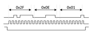
For example ) There is a case where I want to write 0x01 to the FREQ0 register(0x0E) located at the extended address. 

In that case, I transmitted the packet as shown in Figure2 to CC1120 using STM32 to SPI Interface

- Figure 2

It  was confirmed that the above method works when applied to the STM32 HAL_Driver. (By read Partnumber)

However when using LL_Driver, that method did not work.

This is my question, 

1. Is the packet written to the extended register correct?

2. I Attach the LL_Driver Function that I wrote. Thank you for check the code

<LL_Driver code>

void Extend_Resgister_write(uint8_t action_byte, uint8_t register_byte, uint8_t extend_register_byte, uint8_t value_byte)
{
int i=0;

uint8_t TX_Data[4] = {0,};

//uint8_t RX_Data[4] = {0,};

TX_Data[0] = action_byte|register_byte;

TX_Data[1] = extend_register_byte;

TX_Data[2] = value_byte;

LL_GPIO_ResetOutputPin(CS_GPIO_Port, CS_Pin);

for(i=0;i<4;i++)
{
while(!LL_SPI_IsActiveFlag_TXE(SPI1)) {}
LL_SPI_TransmitData8(SPI1, TX_Data[i]);
}

LL_GPIO_SetOutputPin(CS_GPIO_Port, CS_Pin);
}

Looking forward to your advice. Thank you.

Kind regards,

 - Jae-Heyeong Kim

  • Also I Attach the LL_Driver register read Function that I wrote. 

    This function also doesn't work too. Thank you

    void Extend_Resgister_read(uint8_t action_byte, uint8_t register_byte, uint8_t extend_register_byte)
    {
    int i=0;

    uint8_t TX_Data[4] = {0,};

    uint8_t RX_Data[4] = {0,};

    TX_Data[0] = action_byte|register_byte;

    TX_Data[1] = extend_register_byte;

    LL_GPIO_ResetOutputPin(CS_GPIO_Port, CS_Pin);

    for(i=0;i<3;i++)
    {
    while(!LL_SPI_IsActiveFlag_TXE(SPI1)) {}
    LL_SPI_TransmitData8(SPI1, TX_Data[i]);

    while(!LL_SPI_IsActiveFlag_RXNE(SPI1)) {}
    RX_Data[i]=LL_SPI_ReceiveData8(SPI1);
    }

    LL_GPIO_SetOutputPin(CS_GPIO_Port, CS_Pin);

    printf(">> Read_Data : 0x%02x \r\n", RX_Data[2]);
    }

  • A Single Register Access to extended register space consist of the following:

    Command: R/W 0 1 0 1 1 1 1

    Address: A7 A6 A5 A4 A3 A2 A1 A0

    The address of FREQ0 = 0x0E

    If you want to write 0x01 to FREQ0, the following 3 bytes should be output on the SPI:

    0x2F 0x0E 0x01

    Siri

  • Thank you for your kindess. I understand the explanation. Can you give me an example of an extended register?

  • All the registers in this register space is listed in the user guide in section 3.2.1:

    Register Space Access and Extended Register Space Access

    Siri

  • Thank you, My problem is solve thank you very much