This thread has been locked.

If you have a related question, please click the "Ask a related question" button in the top right corner. The newly created question will be automatically linked to this question.

CC1310: How is the LC parameter value in the antenna balun circuit calculated?

Part Number: CC1310

Hi Team,

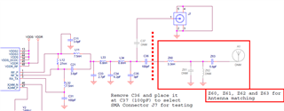
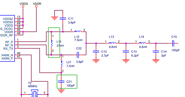
We are clear about the balun circuit and filter circuit of the CC1310 antenna, but the balun circuit here is a little different from the standard circuit in the textbook. There is an extra inductor L11 and an extra capacitor C21, as shown in the green box in the figure.
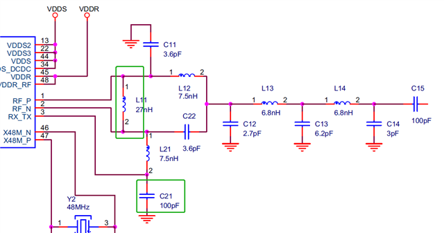
We find that the values ​​of L11 and C21 are different for different frequency antennas (of course, the values ​​of other components are also different, and we know how to pre-calculate the values ​​of other components). But we have the following queries:

1. What are the functions of L11 and C21 here?

2. How could we determine the values ​​of L11 and C21?

I'd appreciate it if you could explain them. Or are there any documents for us to refer to? Thank you in advance.

Kind regards,

Katherine

  • Hi Katherine,

    • L11 = External biasing inductor.
    • C21 = A decoupling capacitor for the RX_TX pin (again as part of the bias network).

    The bias circuit is part of the RF topology; the antenna matching is separate to this (the customer should not need to change the RF section apart from the antenna matching):


    Section 3.1 and Section 9 of SWRA640 (CC13xx/CC26xx Hardware Configuration and PCB Design Considerations): https://www.ti.com/lit/swra640 (particularly Section 9) gives some detail on why we do not recommend for the customer to deviate from the reference design(s).

    The values are found through a combination of theory, simulations, and extensive lab testing/optimisation. The CC1310 itself, the PCB layout, and the components used are some of the factors that can affect this.


    Regards,
    Zack

  • Hi Zack,

    Here is an update of the original question.

    Another customer commented on the original post that the original poster could refer to Section 7.1 of CC1310's specifications, which contented a lot of information and suggested he should refer to TI design when designing the frequency bands. It involved network distribution equipment, RF fine-tuning compensation, etc.

    The original poster replied that Section 7.1 of the CC1310's specifications did not describe how to set the values ​​of L11 and C21. Besides, even if it was "involving network division equipment, RF fine-tuning compensation, etc." (we all have these equipment), TI should also explain how to set the values of L11 and C21 based on these.

    Regards,

    Katherine

  • Hi Zack,

    Below is the reply made by the original poster.

    First of all, thank you for your reply.

    We are very clear about all the circuits except that in the green box in the picture above, including simulation values, project debugging, impedance matching optimization. And we also know the following two points:

    L11 = External biasing inductor.
    C21 = A decoupling capacitor for the RX_TX pin (again as part of the bias network).

    Our question is how to simulate the value of LC in the green box and how to test and optimize it?

    And we can't find any relevant referencing materials.

    The documentation mentioned in your reply doesn't mention this.

    Regards,

    Katherine

  • Hi Zack.

    Below is the replied made by the other customer mentioned earlier.

    TI optimizes the 433/470MHZ drawings, which also involves PCB materials, antenna compensation, etc.

    The relevant content should be aligned accordingly to the actual board, and it is not recommended to make changes considering the reference TI design.

    The original poster added that he was using 433MHZ and 868MHZ.

    Regards,

    Katherine

  • Hi Katherine,


    It is probably useful to know exactly what the customer is trying to do here so that I can give the most relevant information - why do they want to modify the bias inductor value? This is not a component they should need to optimise. We do not recommend modifying the differential section of the RF path.

    If the customer wants to simulate the effect of L11 on the balun (for example if their design differs significantly from the TI reference design), then we recommend simulating the PCB/passive networks of both the TI reference design and the customer's design using ADS or another EDA tool.

    Regards,

    Zack