


Hi all,
I've found on CC3100 layout guide that there is two adviced antennas: AH316M245001-T and RFANT5220110A2T .
I want to ask:
- Since I can see any from datasheet, which difference have this two type of antenna in certifications and performance?
- On RFANT5220110A2T datasheet there is no specified matching components. It's normal? So I don't need to add any antenna components?
- On AH316M245001-T datasheet there is a void but with no specified min. and max. void dimensions, where I can find them?
- In the case of AH316M245001-T I've placed CC3100 in the corner of pcb and I have limited RF wire length, I've calculated wire width to match 50ohm. Since I can't find any min. RF wire lenght, can be good a layout like this? (rectangle is the void, I'll position it better and eliminate vias inside it)
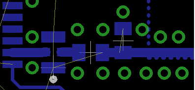
- In CPW-G what is raccomanded via size and distance between vias?
- Should I separate CPW-G Ground from any other components? (or can this improve performace?)
Thank you!
