This thread has been locked.

If you have a related question, please click the "Ask a related question" button in the top right corner. The newly created question will be automatically linked to this question.

CC3200MODLAUNCHXL: Jumper/Pin Question for flashing

Part Number: CC3200MODLAUNCHXL
Other Parts Discussed in Thread: CC3200MOD, CC31XXEMUBOOST, UNIFLASH, ENERGIA, CC3200

Good evening!

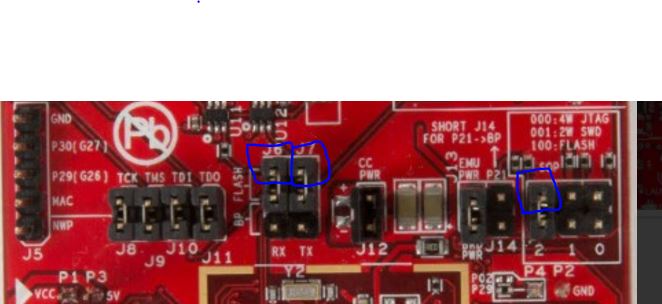
I've got some questions on which pins to use when using the Launchpad to flash a custom PCB. I've tried to find pictures to clarify, but haven't had much luck so far.

For J6 and J7, there are 3 available each. Which do I select?

For SOP2 - which do I select or do I connect both?

Also, my board uses batteries - I assume that I have to have those in for flashing to work, since there's no power input to connect to the Launchpad.


  • Xeeb,

    Have you taken a look at the programmers guide for the CC3200MOD?

    It should answer all the questions you have.

    processors.wiki.ti.com/.../CC3200MOD_Production_Line_Guide

    Let me know if you have any other questions!

    Thanks,

    Vince


  • Yes, I did read it.

    No, it doesn't answer my questions.

    It does show how to use a CC31XXEMUBOOST for UART connection, so I ordered a couple of those.

    While I'm waiting, I'd still like to work with my PCB, so I'd like to know about the specific jumper settings for the Launchpad.

  • Okay.

    See the below picture for reference. You are going to jumper from the emulator side of J6 and J7, and also the high side of SOP2. The blue squares are pins you will need to jumper.


  • Thank you so much!

    Do I also need to remove the jumpers from J8-J11?
  • Yes,

    You can go ahead and disconnect those.

    VR
  • Thank you again.

    Just to summarize, I have removed jumpers from J6-J11, as well as from SOP2.

    I've connected a test lead from RX (J6 on the launchpad) to a lead soldered to a resistor on pin 47 on my PCB.

    I've connected a test lead from TX (J7 on the launchpad) to a lead soldered to a test point on pin 46 on my PCB.

    I've connected a test lead from SOP2 on the launchpad to a lead soldered to a test point on pin 23 on my PCB.

    I've connected the RESET pin from the Launchpad's P16 (in row P2) to a lead soldered to a test point on pin 35 on my PCB.

    I've attached a picture of the current setup.

    Uniflash will not format the serial flash, program the serial flash, or apply a service pack.

    When attempting to debug the basic Getting Started project in CCS7, the debugger stops at 35% of "Launching wlan_station"

    When attempting to upload the "ScanNetworks" sketch in Energia, the "Uploading" progress bar sits at 100% until 3 tries, then it returns "Failed to trigger bootloader"

    All of these functions work when the Launchpad is used by itself.

    Right now, I'm setting up a breadboard with pull up and pull down to give the CC31XXEMUBOOST a try, using the instructions from the Wiki.

  • Xeeb,

    It looks like you are pulling the correct pins off of the launchpad to flash the device over UART. This configuration will only allow you to flash the device, so you will not be able to debug it. (Using Code Composer Studio)

    How do the pins you are connecting to on your PCB correlate to the pins on the CC3200MOD?

    Trying to make sure we are connecting the pins correctly.

    Thanks!

    Vince Rodriguez


  • Thank you! That is an important bit of information that I missed completely!

    Since my last message yesterday, I soldered leads on two more PCBs last night and attached at the solder end.

    I was able to format, apply service pack, and upload OOB firmware to both PCBs. I assume it wrote to the PCB in each case, since it doesn't do so to the Launchpad when I remove the leads but don't put the default jumpers in place.

    As far as debugging, is that done via JTAG? If so, do you recommend using pins J8-J11 from the launchpad?

    My JTAG layout is:

    1 - TDI 2 - VBAT
    3 - TDO 4 - RST
    5 - TCK 6 - GND
    7 - TMS 8 - unused

    So I would just connect J10 to PCB JTAG pin 1, J11 to PCB JTAG pin 3, J8 to PCB JTAG pin 5, and J9 to PCB JTAG pin 7, with connections to reset and ground from the pin rows.

    Alternatively, is there a specific debugger recommended for the CC3200, maybe like the XDS100 v2, to use to connect directly?

    Also, thank you for taking the time to answer these questions. When you search the forum, there are pages and pages of threads, many of them just saying "search the forum, this has already been answered" :)
  • No problem Xeeb!

    Yes if you would like to do JTAG debugging you can use the XDS110 that is available on the launchpad and jumper it over to your board. the jumpers are labeled for each signal you need, and pin closest to the emulator (Big IC on the top of launchpad), is the one connected to the on board emulator.

    I wouldn't say there is any specific emulator you have to use, it is up to you to decide for price/performance. The launchpad comes with the XDS110 which should work fine for you!

    Let me know if you this works for you!

    Thanks,

    Vince Rodriguez


  • That is working for me. The module is connecting to my WiFi and I've got LEDs working.

    Interestingly enough, the two PCBs that I tested for flashing do not work debugging but a third that I never flashed does work.

    Bottom line, I can test the design with the debugger and build a "test" firmware for the first two and see if I have any other issues.

    Thank you again!
  • Thats great news!

    Good luck with your testing and let me know if you have anymore questions!

    Thanks,

    Vince Rodriguez