This thread has been locked.

If you have a related question, please click the "Ask a related question" button in the top right corner. The newly created question will be automatically linked to this question.

CC3220S: Trouble sending data over SPI using DMA

Part Number: CC3220S
Other Parts Discussed in Thread: SYSCONFIG

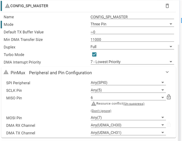
I have been able to successfully transfer data using spi if I set the minimum DMA bytes to something really high, however when I set the min dma transfer size to something smaller as shown in the picture, I keep running into dmaErrorFxn at run time. 

My current spi configurations are shown below:

I would like some help debugging this.

Thanks!

Vasav

  • Hi Vasav,

    If you keep the min DMA transfer size to a higher value, do you encounter any errors?

    The SPI drivers have been tested with the default DMA settings, and changing them to be smaller will cause the DMA to be used more, and also less efficiently if you're performing many small transfers. That being said, 10 bytes as what you've shown should be usable without errors.

    If you use the same settings but run a simple test application such as the spimaster demo, do you still encounter those DMA errors?

    Regards,

    Michael

  • Hi Michael,

    Based on your suggestion I tried a few things out. First, I created a program to test just the spi out itself using the pin configurations required for my board (it is essentially doing the same as the spimasterdemo, except it's reduced to just do TX). In this program, I am sending 100bytes over spi and observing the output using a logic analyzer. When I set the minDMATransfer to 1000 bytes, I can see that all the data is being sent. As shown in the first picture in the.  

    Then I tried to change the minDMATransfer to 10 instead and I noticed that it was getting stuck in freeRTOS functions. I also noticed that some bytes were transferred but not all. Here is the image of what I notice on the logic analyzer.   
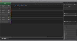
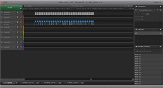
As you can see, only 33 bytes are sent and after that it gets stuck in the freeRTOS stuff. 

    I also temporarily changed the hardware configuration from master Tx only to Full Duplex, and 3 wire to 4 pin SS with active low. Using this configuration I was able to get the code to run with the DMA. So in conclusion I'm not sure what to try next, or what could be causing this issue. 

    Thank you for your help!

    Vasav

  • Hi Vasav,

    It is interesting that you are able to get the correct functionality in full duplex mode.

    If you are able to get the correct functionality in full duplex mode, then I suggest you keep it as so and then perform TX-only transfers by simply specifying NULL as the rxBuf. By doing so you will instruct the driver to use a scratch buffer internally, and it will function as if you are only performing a TX operation.

    Regards,

    Michael

  • Good suggestion Michael,

    Currently, I can't keep it in full-duplex mode because it causes resource conflict in the sys config. Is there a way around this problem?

    Thanks for your help!

  • Hi Vasav,

    What pin conflict do you have with the SPI RX pin? Perhaps there is a way to work around it, though I'll need to know what other peripheral is taking up the same pin.

    Regards,

    Michael

  • Hey Michael,

    In my hardware, I have a mux being controlled the SPI RX pin by using it as a GPIO pin instead. I was able to suppress the pin conflict and then get the DMA to work when I put the SPI mode as full-duplex. To do this, I had to lock the RX pin and then I was given the option to suppress the error. 

    I think it would still be beneficial if someone can figure out why only the full-duplex version works with the DMA.

    Thanks!

    Vasav

  • Hi Vasav,

    I agree that it would be best if we could debug and determine why the half-duplex mode is unstable when used with DMA.

    It is however good to know that you have figured out a workaround for your pin conflict. Unfortunately I don't think I will be able to allocate further time to debug this issue, especially given we have a workaround that works.

    Let me know if you have further questions about the SPI driver.

    Regards,

    Michael

  • Hey Michael,

    Although this is temporarily working is it possible for you to have another engineer take a deeper look into why the dma requires a full-duplex mode and how to go about fixing my original issue? I am asking because it is highly likely the GPIO needs to be used at the same as the SPI and this scenario will cause problems. 

    Thanks!

    Vasav 

  • Hi Vasav,

    Along with the full duplex change, did you also have to use 4 wire SPI mode, or were you also able to use 3 wire SPI once you had full duplex enabled?

    Regards,

    Michael

  • HI Michael,

    I was able to use 3 wire SPI once I had the full-duplex enabled. These are the settings for the SPI in my sysconfig for your reference.

    Thanks!

    Vasav

  • I realized in the image above the minDMA is much larger (I forgot to switch branches), the other branch has about 100 bytes for minDMA transfer size. 

  • Hi Vasav,

    Thanks for providing that screenshot of your sysconfig SPI setup.

    I have a few more clarifying questions:

    1. When you perform the half-duplex tests, what is the transfer count you use? Specifically, does the issue always occur when the .count > min DMA transfer size? Keep in mind that both count and min DMA transfer size are in SPI words (so 8 bytes if you're running 8 bytes per word, etc)

    2. When you run half-duplex SPI and attempt to perform a transfer, do you leave the rxbuf as NULL, or do you still provide a buffer to the SPI_Transfer() function?

    3. Does the issue occur on the first SPI_Transfer(), or only on the second + SPI transfer.

    What might be happening is that the DMA transfer setup does not interact with the SPI peripheral correctly if the SPI is in half-duplex. Specifically it's trying to fetch data from a FIFO that isn't getting filled. What happens if you modify the SPI driver to disable the DMA setup for the disabled TX or RX? I've attached a modified driver that attempts to do just that, please give a try - I unfortunately do not have the bandwidth to fully test out this idea, so your help here would be appreciated.

    3312.SPICC32XXDMA.c
    /*
     * Copyright (c) 2015-2018, Texas Instruments Incorporated
     * All rights reserved.
     *
     * Redistribution and use in source and binary forms, with or without
     * modification, are permitted provided that the following conditions
     * are met:
     *
     * *  Redistributions of source code must retain the above copyright
     *    notice, this list of conditions and the following disclaimer.
     *
     * *  Redistributions in binary form must reproduce the above copyright
     *    notice, this list of conditions and the following disclaimer in the
     *    documentation and/or other materials provided with the distribution.
     *
     * *  Neither the name of Texas Instruments Incorporated nor the names of
     *    its contributors may be used to endorse or promote products derived
     *    from this software without specific prior written permission.
     *
     * THIS SOFTWARE IS PROVIDED BY THE COPYRIGHT HOLDERS AND CONTRIBUTORS "AS IS"
     * AND ANY EXPRESS OR IMPLIED WARRANTIES, INCLUDING, BUT NOT LIMITED TO,
     * THE IMPLIED WARRANTIES OF MERCHANTABILITY AND FITNESS FOR A PARTICULAR
     * PURPOSE ARE DISCLAIMED. IN NO EVENT SHALL THE COPYRIGHT OWNER OR
     * CONTRIBUTORS BE LIABLE FOR ANY DIRECT, INDIRECT, INCIDENTAL, SPECIAL,
     * EXEMPLARY, OR CONSEQUENTIAL DAMAGES (INCLUDING, BUT NOT LIMITED TO,
     * PROCUREMENT OF SUBSTITUTE GOODS OR SERVICES; LOSS OF USE, DATA, OR PROFITS;
     * OR BUSINESS INTERRUPTION) HOWEVER CAUSED AND ON ANY THEORY OF LIABILITY,
     * WHETHER IN CONTRACT, STRICT LIABILITY, OR TORT (INCLUDING NEGLIGENCE OR
     * OTHERWISE) ARISING IN ANY WAY OUT OF THE USE OF THIS SOFTWARE,
     * EVEN IF ADVISED OF THE POSSIBILITY OF SUCH DAMAGE.
     */
    #include <stdbool.h>
    #include <stddef.h>
    #include <stdint.h>
    
    #include <ti/devices/cc32xx/inc/hw_mcspi.h>
    #include <ti/devices/cc32xx/inc/hw_types.h>
    #include <ti/devices/cc32xx/inc/hw_memmap.h>
    #include <ti/devices/cc32xx/inc/hw_udma.h>
    #include <ti/devices/cc32xx/inc/hw_ocp_shared.h>
    #include <ti/devices/cc32xx/driverlib/rom.h>
    #include <ti/devices/cc32xx/driverlib/rom_map.h>
    #include <ti/devices/cc32xx/driverlib/prcm.h>
    #include <ti/devices/cc32xx/driverlib/spi.h>
    #include <ti/devices/cc32xx/driverlib/udma.h>
    
    #include <ti/drivers/dma/UDMACC32XX.h>
    #include <ti/drivers/dpl/HwiP.h>
    #include <ti/drivers/dpl/SemaphoreP.h>
    #include <ti/drivers/Power.h>
    #include <ti/drivers/power/PowerCC32XX.h>
    #include <ti/drivers/spi/SPICC32XXDMA.h>
    
    #define MAX_DMA_TRANSFER_AMOUNT (1024)
    
    #define PAD_CONFIG_BASE (OCP_SHARED_BASE + OCP_SHARED_O_GPIO_PAD_CONFIG_0)
    #define PAD_RESET_STATE 0xC61
    
    void SPICC32XXDMA_close(SPI_Handle handle);
    int_fast16_t SPICC32XXDMA_control(SPI_Handle handle, uint_fast16_t cmd,
        void *arg);
    void SPICC32XXDMA_init(SPI_Handle handle);
    SPI_Handle SPICC32XXDMA_open(SPI_Handle handle, SPI_Params *params);
    bool SPICC32XXDMA_transfer(SPI_Handle handle, SPI_Transaction *transaction);
    void SPICC32XXDMA_transferCancel(SPI_Handle handle);
    
    /* SPI function table for SPICC32XXDMA implementation */
    const SPI_FxnTable SPICC32XXDMA_fxnTable = {
        SPICC32XXDMA_close,
        SPICC32XXDMA_control,
        SPICC32XXDMA_init,
        SPICC32XXDMA_open,
        SPICC32XXDMA_transfer,
        SPICC32XXDMA_transferCancel
    };
    
    static const uint32_t mode[] = {
        SPI_MODE_MASTER,
        SPI_MODE_SLAVE
    };
    
    /*
     * This lookup table is used to configure the DMA channels for the appropriate
     * (8bit, 16bit or 32bit) transfer sizes.
     * Table for an SPI DMA RX channel.
     */
    static const uint32_t dmaRxConfig[] = {
        UDMA_SIZE_8  | UDMA_SRC_INC_NONE | UDMA_DST_INC_8  | UDMA_ARB_1,
        UDMA_SIZE_16 | UDMA_SRC_INC_NONE | UDMA_DST_INC_16 | UDMA_ARB_1,
        UDMA_SIZE_32 | UDMA_SRC_INC_NONE | UDMA_DST_INC_32 | UDMA_ARB_1
    };
    
    /*
     * This lookup table is used to configure the DMA channels for the appropriate
     * (8bit, 16bit or 32bit) transfer sizes.
     * Table for an SPI DMA TX channel
     */
    static const uint32_t dmaTxConfig[] = {
        UDMA_SIZE_8  | UDMA_SRC_INC_8  | UDMA_DST_INC_NONE | UDMA_ARB_1,
        UDMA_SIZE_16 | UDMA_SRC_INC_16 | UDMA_DST_INC_NONE | UDMA_ARB_1,
        UDMA_SIZE_32 | UDMA_SRC_INC_32 | UDMA_DST_INC_NONE | UDMA_ARB_1
    };
    
    /*
     * This lookup table is used to configure the DMA channels for the appropriate
     * (8bit, 16bit or 32bit) transfer sizes when either txBuf or rxBuf are NULL.
     */
    static const uint32_t dmaNullConfig[] = {
        UDMA_SIZE_8  | UDMA_SRC_INC_NONE | UDMA_DST_INC_NONE | UDMA_ARB_1,
        UDMA_SIZE_16 | UDMA_SRC_INC_NONE | UDMA_DST_INC_NONE | UDMA_ARB_1,
        UDMA_SIZE_32 | UDMA_SRC_INC_NONE | UDMA_DST_INC_NONE | UDMA_ARB_1
    };
    
    /*
     *  ======== blockingTransferCallback ========
     */
    static void blockingTransferCallback(SPI_Handle handle,
        SPI_Transaction *transaction)
    {
        SPICC32XXDMA_Object *object = handle->object;
    
        SemaphoreP_post(object->transferComplete);
    }
    
    /*
     *  ======== configDMA ========
     *  This functions configures the transmit and receive DMA channels for a given
     *  SPI_Handle and SPI_Transaction
     */
    static void configDMA(SPICC32XXDMA_Object *object,
        SPICC32XXDMA_HWAttrsV1 const *hwAttrs, SPI_Transaction *transaction)
    {
        uintptr_t  key;
        void      *buf;
        uint32_t   channelControlOptions;
        uint8_t    dataFrameSizeInBytes;
        uint8_t    optionsIndex;
    
        /* DMA options used vary according to data size. */
        if (object->dataSize < 9) {
            optionsIndex = 0;
            dataFrameSizeInBytes = sizeof(uint8_t);
        }
        else if (object->dataSize < 17) {
            optionsIndex = 1;
            dataFrameSizeInBytes = sizeof(uint16_t);;
        }
        else {
            optionsIndex = 2;
            dataFrameSizeInBytes = sizeof(uint32_t);
        }
    
        /*
         * The DMA has a max transfer amount of 1024.  If the transaction is
         * greater; we must transfer it in chunks.  object->amtDataXferred has
         * how much data has already been sent.
         */
        if ((transaction->count - object->amtDataXferred) > MAX_DMA_TRANSFER_AMOUNT) {
            object->currentXferAmt = MAX_DMA_TRANSFER_AMOUNT;
        }
        else {
            object->currentXferAmt = (transaction->count - object->amtDataXferred);
        }
    
    	if(hwAttrs->mosiPin != SPICC32XXDMA_PIN_NO_CONFIG){
    		if (transaction->txBuf) {
    			channelControlOptions = dmaTxConfig[optionsIndex];
    			/*
    			 * Add an offset for the amount of data transfered.  The offset is
    			 * calculated by: object->amtDataXferred * (dataFrameSizeInBytes).
    			 * This accounts for 8, 16 or 32-bit sized transfers.
    			 */
    			buf = (void *) ((uint32_t) transaction->txBuf +
    				((uint32_t) object->amtDataXferred * dataFrameSizeInBytes));
    		}
    		else {
    			channelControlOptions = dmaNullConfig[optionsIndex];
    			*hwAttrs->scratchBufPtr = hwAttrs->defaultTxBufValue;
    			buf = hwAttrs->scratchBufPtr;
    		}
    
    		/* Setup the TX transfer characteristics & buffers */
    		MAP_uDMAChannelControlSet(hwAttrs->txChannelIndex | UDMA_PRI_SELECT,
    			channelControlOptions);
    		MAP_uDMAChannelAttributeDisable(hwAttrs->txChannelIndex,
    			UDMA_ATTR_ALTSELECT);
    		MAP_uDMAChannelTransferSet(hwAttrs->txChannelIndex | UDMA_PRI_SELECT,
    			UDMA_MODE_BASIC, buf, (void *) (hwAttrs->baseAddr + MCSPI_O_TX0),
    			object->currentXferAmt);
    	}
    	if(hwAttrs->misoPin != SPICC32XXDMA_PIN_NO_CONFIG){
    		if (transaction->rxBuf) {
    			channelControlOptions = dmaRxConfig[optionsIndex];
    			/*
    			 * Add an offset for the amount of data transfered.  The offset is
    			 * calculated by: object->amtDataXferred * (dataFrameSizeInBytes).
    			 * This accounts for 8 or 16-bit sized transfers.
    			 */
    			buf = (void *) ((uint32_t) transaction->rxBuf +
    				((uint32_t) object->amtDataXferred * dataFrameSizeInBytes));
    		}
    		else {
    			channelControlOptions = dmaNullConfig[optionsIndex];
    			buf = hwAttrs->scratchBufPtr;
    		}
    
    		/* Setup the RX transfer characteristics & buffers */
    		MAP_uDMAChannelControlSet(hwAttrs->rxChannelIndex | UDMA_PRI_SELECT,
    			channelControlOptions);
    		MAP_uDMAChannelAttributeDisable(hwAttrs->rxChannelIndex,
    			UDMA_ATTR_ALTSELECT);
    		MAP_uDMAChannelTransferSet(hwAttrs->rxChannelIndex | UDMA_PRI_SELECT,
    			UDMA_MODE_BASIC, (void *) (hwAttrs->baseAddr + MCSPI_O_RX0), buf,
    			object->currentXferAmt);
    	}
        /* A lock is needed because we are accessing shared uDMA memory */
        key = HwiP_disable();
    
        /*
         * DMA channels 30 and 31 are connected to the SPI peripheral by default.
         * If someone hasn't remapped them to something else already, we remap
         * them to SW.
         */
        if (!(HWREG(UDMA_BASE + UDMA_O_CHMAP3) & UDMA_CHMAP3_CH30SEL_M)) {
            MAP_uDMAChannelAssign(UDMA_CH30_SW);
        }
        if (!(HWREG(UDMA_BASE + UDMA_O_CHMAP3) & UDMA_CHMAP3_CH31SEL_M)) {
            MAP_uDMAChannelAssign(UDMA_CH31_SW);
        }
    
        /* Assign the requested DMA channels */
        MAP_uDMAChannelAssign(hwAttrs->rxChannelIndex);
        MAP_uDMAChannelAssign(hwAttrs->txChannelIndex);
    
        /* Enable DMA to generate interrupt on SPI peripheral */
    	if(hwAttrs->mosiPin != SPICC32XXDMA_PIN_NO_CONFIG){
    		MAP_SPIDmaEnable(hwAttrs->baseAddr, SPI_TX_DMA);
    	}
    	if(hwAttrs->misoPin != SPICC32XXDMA_PIN_NO_CONFIG){
    		MAP_SPIDmaEnable(hwAttrs->baseAddr, SPI_RX_DMA);
    	}
        MAP_SPIIntClear(hwAttrs->baseAddr, SPI_INT_DMATX|SPI_INT_DMARX);
        MAP_SPIIntEnable(hwAttrs->baseAddr, SPI_INT_EOW);
        MAP_SPIWordCountSet(hwAttrs->baseAddr, object->currentXferAmt);
    
        /* Enable channels & start DMA transfers */
        MAP_uDMAChannelEnable(hwAttrs->txChannelIndex);
        MAP_uDMAChannelEnable(hwAttrs->rxChannelIndex);
    
        HwiP_restore(key);
    
        MAP_SPIEnable(hwAttrs->baseAddr);
        MAP_SPICSEnable(hwAttrs->baseAddr);
    }
    
    /*
     *  ======== getDmaRemainingXfers ========
     */
    static inline uint32_t getDmaRemainingXfers(SPICC32XXDMA_HWAttrsV1 const *hwAttrs) {
        uint32_t          controlWord;
        tDMAControlTable *controlTable;
    
        controlTable = MAP_uDMAControlBaseGet();
        controlWord = controlTable[(hwAttrs->rxChannelIndex & 0x3f)].ulControl;
    
        return (((controlWord & UDMA_CHCTL_XFERSIZE_M) >> 4) + 1);
    }
    
    /*
     *  ======== getPowerMgrId ========
     */
    static uint16_t getPowerMgrId(uint32_t baseAddr)
    {
        switch (baseAddr) {
            case GSPI_BASE:
                return (PowerCC32XX_PERIPH_GSPI);
            case LSPI_BASE:
                return (PowerCC32XX_PERIPH_LSPI);
            default:
                return (~0);
        }
    }
    
    /*
     *  ======== initHw ========
     */
    static void initHw(SPICC32XXDMA_Object *object,
        SPICC32XXDMA_HWAttrsV1 const *hwAttrs)
    {
        /*
         * SPI peripheral should remain disabled until a transfer is requested.
         * This is done to prevent the RX FIFO from gathering data from other
         * transfers.
         */
        MAP_SPICSDisable(hwAttrs->baseAddr);
        MAP_SPIDisable(hwAttrs->baseAddr);
        MAP_SPIReset(hwAttrs->baseAddr);
    
        MAP_SPIConfigSetExpClk(hwAttrs->baseAddr,
            MAP_PRCMPeripheralClockGet(hwAttrs->spiPRCM), object->bitRate,
            mode[object->spiMode], object->frameFormat,
            (hwAttrs->csControl | hwAttrs->pinMode | hwAttrs->turboMode |
            hwAttrs->csPolarity | ((object->dataSize - 1) << 7)));
    
        MAP_SPIFIFOEnable(hwAttrs->baseAddr, SPI_RX_FIFO | SPI_TX_FIFO);
        MAP_SPIFIFOLevelSet(hwAttrs->baseAddr, object->txFifoTrigger,
            object->rxFifoTrigger);
    }
    
    /*
     *  ======== postNotifyFxn ========
     */
    static int postNotifyFxn(unsigned int eventType, uintptr_t eventArg,
        uintptr_t clientArg)
    {
        SPICC32XXDMA_Object          *object = ((SPI_Handle) clientArg)->object;
        SPICC32XXDMA_HWAttrsV1 const *hwAttrs = ((SPI_Handle) clientArg)->hwAttrs;
    
        initHw(object, hwAttrs);
    
        return (Power_NOTIFYDONE);
    }
    
    /*
     *  ======== spiHwiFxn ========
     */
    static void spiHwiFxn(uintptr_t arg)
    {
        uint32_t                      intFlags;
        SPI_Transaction              *msg;
        SPICC32XXDMA_Object          *object = ((SPI_Handle)arg)->object;
        SPICC32XXDMA_HWAttrsV1 const *hwAttrs = ((SPI_Handle)arg)->hwAttrs;
    
        /*
         * Although the DMATX interrupt is not used by this driver, it seems like
         * it is still triggering DMA interrupts.  The code below will clear &
         * disable the interrupt thus reducing the amount of spurious interrupts.
         */
        intFlags = MAP_SPIIntStatus(hwAttrs->baseAddr, false);
        if (intFlags & SPI_INT_DMATX) {
            MAP_SPIIntDisable(hwAttrs->baseAddr, SPI_INT_DMATX);
            MAP_SPIIntClear(hwAttrs->baseAddr, SPI_INT_DMATX);
        }
        if (intFlags & SPI_INT_DMARX) {
            MAP_SPIIntDisable(hwAttrs->baseAddr, SPI_INT_DMARX);
            MAP_SPIIntClear(hwAttrs->baseAddr, SPI_INT_DMARX);
        }
    //    if (MAP_uDMAChannelIsEnabled(hwAttrs->rxChannelIndex)) {
    //        /* DMA has not completed if the channel is still enabled */
    //        return;
    //   }
    
        /* EOW condition has been met - transfer has completed; disable peripheral */
        MAP_SPIDmaDisable(hwAttrs->baseAddr, SPI_RX_DMA | SPI_TX_DMA);
        MAP_SPIIntDisable(hwAttrs->baseAddr, SPI_INT_EOW|SPI_INT_DMARX);
        MAP_SPIIntClear(hwAttrs->baseAddr, SPI_INT_EOW|SPI_INT_DMARX);
        MAP_SPICSDisable(hwAttrs->baseAddr);
        MAP_SPIDisable(hwAttrs->baseAddr);
    
        if (object->transaction->count - object->amtDataXferred >
            MAX_DMA_TRANSFER_AMOUNT) {
            /* Data still remaining, configure another DMA transfer */
            object->amtDataXferred += object->currentXferAmt;
    
            configDMA(object, hwAttrs, object->transaction);
        }
        else {
            /* All data sent; set status, perform callback & return */
            object->transaction->status = SPI_TRANSFER_COMPLETED;
    
            /* Release constraint since transaction is done */
            Power_releaseConstraint(PowerCC32XX_DISALLOW_LPDS);
    
            /*
             * Use a temporary transaction pointer in case the callback function
             * attempts to perform another SPI_transfer call
             */
            msg = object->transaction;
    
            /* Indicate we are done with this transfer */
            object->transaction = NULL;
    
            object->transferCallbackFxn((SPI_Handle) arg, msg);
        }
    }
    
    /*
     *  ======== spiPollingTransfer ========
     */
    static inline void spiPollingTransfer(SPICC32XXDMA_Object *object,
        SPICC32XXDMA_HWAttrsV1 const *hwAttrs, SPI_Transaction *transaction)
    {
        uint8_t   increment;
        uint32_t  dummyBuffer;
        size_t    transferCount;
        void     *rxBuf;
        void     *txBuf;
    
        if (transaction->rxBuf) {
            rxBuf = transaction->rxBuf;
        }
        else {
            rxBuf = hwAttrs->scratchBufPtr;
        }
    
        if (transaction->txBuf) {
            txBuf = transaction->txBuf;
        }
        else {
            *hwAttrs->scratchBufPtr = hwAttrs->defaultTxBufValue;
            txBuf = hwAttrs->scratchBufPtr;
        }
    
        if (object->dataSize < 9) {
            increment = sizeof(uint8_t);
        }
        else if (object->dataSize < 17) {
            increment = sizeof(uint16_t);
        }
        else {
            increment = sizeof(uint32_t);
        }
    
        transferCount = transaction->count;
    
        /*
         * Start the polling transfer - we MUST set word count to 0; not doing so
         * will raise spurious RX interrupts flags (though interrupts are not
         * enabled).
         */
        MAP_SPIWordCountSet(hwAttrs->baseAddr, 0);
        MAP_SPIEnable(hwAttrs->baseAddr);
        MAP_SPICSEnable(hwAttrs->baseAddr);
    
        while (transferCount--) {
            if (object->dataSize < 9) {
                MAP_SPIDataPut(hwAttrs->baseAddr, *((uint8_t *) txBuf));
                MAP_SPIDataGet(hwAttrs->baseAddr, (unsigned long *)&dummyBuffer);
                *((uint8_t *) rxBuf) = (uint8_t) dummyBuffer;
            }
            else if (object->dataSize < 17) {
                MAP_SPIDataPut(hwAttrs->baseAddr, *((uint16_t *) txBuf));
                MAP_SPIDataGet(hwAttrs->baseAddr, (unsigned long *) &dummyBuffer);
                *((uint16_t *) rxBuf) = (uint16_t) dummyBuffer;
            }
            else {
                MAP_SPIDataPut(hwAttrs->baseAddr, *((uint32_t *) txBuf));
                MAP_SPIDataGet(hwAttrs->baseAddr, (unsigned long * ) rxBuf);
            }
    
            /* Only increment source & destination if buffers were provided */
            if (transaction->rxBuf) {
                rxBuf = (void *) (((uint32_t) rxBuf) + increment);
            }
            if (transaction->txBuf) {
                txBuf = (void *) (((uint32_t) txBuf) + increment);
            }
        }
    
        MAP_SPICSDisable(hwAttrs->baseAddr);
        MAP_SPIDisable(hwAttrs->baseAddr);
    }
    
    /*
     *  ======== SPICC32XXDMA_close ========
     */
    void SPICC32XXDMA_close(SPI_Handle handle)
    {
        uint32_t                      padRegister;
        SPICC32XXDMA_Object          *object = handle->object;
        SPICC32XXDMA_HWAttrsV1 const *hwAttrs = handle->hwAttrs;
    
        MAP_SPICSDisable(hwAttrs->baseAddr);
        MAP_SPIDisable(hwAttrs->baseAddr);
        MAP_SPIFIFODisable(hwAttrs->baseAddr, SPI_RX_FIFO | SPI_TX_FIFO);
    
        /* Release power dependency on SPI. */
        Power_releaseDependency(getPowerMgrId(hwAttrs->baseAddr));
        Power_unregisterNotify(&(object->notifyObj));
    
        if (object->hwiHandle) {
            HwiP_delete(object->hwiHandle);
            object->hwiHandle = NULL;
        }
        if (object->transferComplete) {
            SemaphoreP_delete(object->transferComplete);
            object->transferComplete = NULL;
        }
    
        if (object->dmaHandle) {
            UDMACC32XX_close(object->dmaHandle);
            object->dmaHandle = NULL;
        }
    
        /* Restore pin pads to their reset states */
        if (hwAttrs->mosiPin != SPICC32XXDMA_PIN_NO_CONFIG) {
            padRegister = (PinToPadGet((hwAttrs->mosiPin) & 0xff)<<2)
                + PAD_CONFIG_BASE;
            HWREG(padRegister) = PAD_RESET_STATE;
        }
        if (hwAttrs->misoPin != SPICC32XXDMA_PIN_NO_CONFIG) {
            padRegister = (PinToPadGet((hwAttrs->misoPin) & 0xff)<<2)
                + PAD_CONFIG_BASE;
            HWREG(padRegister) = PAD_RESET_STATE;
        }
        if (hwAttrs->clkPin != SPICC32XXDMA_PIN_NO_CONFIG) {
            padRegister = (PinToPadGet((hwAttrs->clkPin) & 0xff)<<2)
                + PAD_CONFIG_BASE;
            HWREG(padRegister) = PAD_RESET_STATE;
        }
        if ((hwAttrs->pinMode == SPI_4PIN_MODE) &&
            (hwAttrs->csPin != SPICC32XXDMA_PIN_NO_CONFIG)) {
            padRegister = (PinToPadGet((hwAttrs->csPin) & 0xff)<<2)
                + PAD_CONFIG_BASE;
            HWREG(padRegister) = PAD_RESET_STATE;
        }
    
        object->isOpen = false;
    }
    
    /*
     *  ======== SPICC32XXDMA_control ========
     */
    int_fast16_t SPICC32XXDMA_control(SPI_Handle handle, uint_fast16_t cmd, void *arg)
    {
        return (SPI_STATUS_UNDEFINEDCMD);
    }
    
    /*
     *  ======== SPICC32XXDMA_init ========
     */
    void SPICC32XXDMA_init(SPI_Handle handle)
    {
        UDMACC32XX_init();
    }
    
    /*
     *  ======== SPICC32XXDMA_open ========
     */
    SPI_Handle SPICC32XXDMA_open(SPI_Handle handle, SPI_Params *params)
    {
        uintptr_t                     key;
        uint16_t                      pin;
        uint16_t                      mode;
        uint8_t                       powerMgrId;
        HwiP_Params                   hwiParams;
        SPICC32XXDMA_Object          *object = handle->object;
        SPICC32XXDMA_HWAttrsV1 const *hwAttrs = handle->hwAttrs;
    
        key = HwiP_disable();
    
        if (object->isOpen) {
            HwiP_restore(key);
    
            return (NULL);
        }
        object->isOpen = true;
    
        HwiP_restore(key);
    
        /* SPI_TI & SPI_MW are not supported */
        if (params->frameFormat == SPI_TI || params->frameFormat == SPI_MW) {
            object->isOpen = false;
    
            return (NULL);
        }
    
        /* Register power dependency - i.e. power up and enable clock for SPI. */
        powerMgrId = getPowerMgrId(hwAttrs->baseAddr);
        if (powerMgrId > PowerCC32XX_NUMRESOURCES) {
            object->isOpen = false;
    
            return (NULL);
        }
        Power_setDependency(powerMgrId);
        Power_registerNotify(&(object->notifyObj), PowerCC32XX_AWAKE_LPDS,
            postNotifyFxn, (uintptr_t) handle);
    
        /* Configure the pins */
        if (hwAttrs->mosiPin != SPICC32XXDMA_PIN_NO_CONFIG) {
            pin = (hwAttrs->mosiPin) & 0xff;
            mode = (hwAttrs->mosiPin >> 8) & 0xff;
            MAP_PinTypeSPI((unsigned long) pin, (unsigned long) mode);
        }
    
        if (hwAttrs->misoPin != SPICC32XXDMA_PIN_NO_CONFIG) {
            pin = (hwAttrs->misoPin) & 0xff;
            mode = (hwAttrs->misoPin >> 8) & 0xff;
            MAP_PinTypeSPI((unsigned long) pin, (unsigned long) mode);
        }
    
        if (hwAttrs->clkPin != SPICC32XXDMA_PIN_NO_CONFIG) {
            pin = (hwAttrs->clkPin) & 0xff;
            mode = (hwAttrs->clkPin >> 8) & 0xff;
            MAP_PinTypeSPI((unsigned long) pin, (unsigned long) mode);
        }
    
        if (hwAttrs->pinMode == SPI_4PIN_MODE) {
            if (hwAttrs->csPin != SPICC32XXDMA_PIN_NO_CONFIG) {
                pin = (hwAttrs->csPin) & 0xff;
                mode = (hwAttrs->csPin >> 8) & 0xff;
                MAP_PinTypeSPI((unsigned long) pin, (unsigned long) mode);
            }
        }
    
        object->dmaHandle = UDMACC32XX_open();
        if (object->dmaHandle == NULL) {
            SPICC32XXDMA_close(handle);
    
            return (NULL);
        }
    
        HwiP_Params_init(&hwiParams);
        hwiParams.arg = (uintptr_t) handle;
        hwiParams.priority = hwAttrs->intPriority;
        object->hwiHandle = HwiP_create(hwAttrs->intNum, spiHwiFxn, &hwiParams);
        if (object->hwiHandle == NULL) {
            SPICC32XXDMA_close(handle);
    
            return (NULL);
        }
    
        if (params->transferMode == SPI_MODE_BLOCKING) {
            /*
             * Create a semaphore to block task execution for the duration of the
             * SPI transfer
             */
            object->transferComplete = SemaphoreP_createBinary(0);
            if (object->transferComplete == NULL) {
                SPICC32XXDMA_close(handle);
    
                return (NULL);
            }
    
            object->transferCallbackFxn = blockingTransferCallback;
        }
        else {
            if (params->transferCallbackFxn == NULL) {
                SPICC32XXDMA_close(handle);
    
                return (NULL);
            }
    
            object->transferCallbackFxn = params->transferCallbackFxn;
        }
    
        object->bitRate = params->bitRate;
        object->dataSize = params->dataSize;
        object->frameFormat = params->frameFormat;
        object->spiMode = params->mode;
        object->transaction = NULL;
        object->transferMode = params->transferMode;
        object->transferTimeout = params->transferTimeout;
    
        /* SPI FIFO trigger sizes vary based on data frame size */
        if (object->dataSize < 9) {
            object->rxFifoTrigger = sizeof(uint8_t);
            object->txFifoTrigger = sizeof(uint8_t);
        }
        else if (object->dataSize < 17) {
            object->rxFifoTrigger = sizeof(uint16_t);
            object->txFifoTrigger = sizeof(uint16_t);
        }
        else {
            object->rxFifoTrigger = sizeof(uint32_t);
            object->txFifoTrigger = sizeof(uint32_t);
        }
    
        initHw(object, hwAttrs);
    
        return (handle);
    }
    
    /*
     *  ======== SPICC32XXDMA_transfer ========
     */
    bool SPICC32XXDMA_transfer(SPI_Handle handle, SPI_Transaction *transaction)
    {
        uintptr_t                     key;
        uint8_t                       alignMask;
        bool                          buffersAligned;
        SPICC32XXDMA_Object          *object = handle->object;
        SPICC32XXDMA_HWAttrsV1 const *hwAttrs = handle->hwAttrs;
    
        if ((transaction->count == 0) ||
            (transaction->rxBuf == NULL && transaction->txBuf == NULL) ||
            (hwAttrs->scratchBufPtr == NULL && (transaction->rxBuf == NULL ||
                transaction->txBuf == NULL))) {
            return (false);
        }
    
        key = HwiP_disable();
    
        /*
         * alignMask is used to determine if the RX/TX buffers addresses are
         * aligned to the data frame size.
         */
        alignMask = (object->rxFifoTrigger - 1);
        buffersAligned = ((((uint32_t) transaction->rxBuf & alignMask) == 0) &&
            (((uint32_t) transaction->txBuf & alignMask) == 0));
    
        if (object->transaction) {
            HwiP_restore(key);
    
            return (false);
        }
        else {
            object->transaction = transaction;
            object->transaction->status = SPI_TRANSFER_STARTED;
            object->amtDataXferred = 0;
            object->currentXferAmt = 0;
        }
    
        HwiP_restore(key);
    
        /* Set constraints to guarantee transaction */
        Power_setConstraint(PowerCC32XX_DISALLOW_LPDS);
    
        /* Polling transfer if BLOCKING mode & transaction->count < threshold */
        if ((object->transferMode == SPI_MODE_BLOCKING &&
            transaction->count < hwAttrs->minDmaTransferSize) || !buffersAligned) {
            spiPollingTransfer(object, hwAttrs, transaction);
    
            /* Transaction completed; set status & mark SPI ready */
            object->transaction->status = SPI_TRANSFER_COMPLETED;
            object->transaction = NULL;
    
            Power_releaseConstraint(PowerCC32XX_DISALLOW_LPDS);
        }
        else {
            /* Perform a DMA backed SPI transfer */
            configDMA(object, hwAttrs, transaction);
    
            if (object->transferMode == SPI_MODE_BLOCKING) {
                if (SemaphoreP_pend(object->transferComplete,
                    object->transferTimeout) != SemaphoreP_OK) {
                    /* Timeout occurred; cancel the transfer */
                    object->transaction->status = SPI_TRANSFER_FAILED;
                    SPICC32XXDMA_transferCancel(handle);
    
                    /*
                     * TransferCancel() performs callback which posts
                     * transferComplete semaphore. This call consumes this extra post.
                     */
                    SemaphoreP_pend(object->transferComplete, SemaphoreP_NO_WAIT);
    
                    return (false);
                }
            }
        }
    
        return (true);
    }
    
    /*
     *  ======== SPICC32XXDMA_transferCancel ========
     */
    void SPICC32XXDMA_transferCancel(SPI_Handle handle)
    {
        uintptr_t                     key;
        SPI_Transaction              *msg;
        SPICC32XXDMA_Object          *object = handle->object;
        SPICC32XXDMA_HWAttrsV1 const *hwAttrs = handle->hwAttrs;
    
        /*
         * There are 2 use cases in which to call transferCancel():
         *   1.  The driver is in CALLBACK mode.
         *   2.  The driver is in BLOCKING mode & there has been a transfer timeout.
         */
        if (object->transferMode == SPI_MODE_CALLBACK ||
            object->transaction->status == SPI_TRANSFER_FAILED) {
    
            key = HwiP_disable();
    
            if (object->transaction == NULL || object->cancelInProgress) {
                HwiP_restore(key);
    
                return;
            }
            object->cancelInProgress = true;
    
            /* Prevent interrupt from occurring while canceling the transfer */
            HwiP_disableInterrupt(hwAttrs->intNum);
            HwiP_clearInterrupt(hwAttrs->intNum);
    
            /* Clear DMA configuration */
            MAP_uDMAChannelDisable(hwAttrs->rxChannelIndex);
            MAP_uDMAChannelDisable(hwAttrs->txChannelIndex);
    
            MAP_SPIIntDisable(hwAttrs->baseAddr, SPI_INT_DMARX);
            MAP_SPIIntClear(hwAttrs->baseAddr, SPI_INT_DMARX);
            MAP_SPIDmaDisable(hwAttrs->baseAddr, SPI_RX_DMA | SPI_TX_DMA);
    
            HwiP_restore(key);
    
            /*
             * Disables peripheral, clears all registers & reinitializes it to
             * parameters used in SPI_open()
             */
            initHw(object, hwAttrs);
    
            HwiP_enableInterrupt(hwAttrs->intNum);
    
            /*
             * Calculate amount of data which has already been sent & store
             * it in transaction->count
             */
            object->transaction->count = object->amtDataXferred +
                (object->currentXferAmt - getDmaRemainingXfers(hwAttrs));
    
            /* Set status CANCELED if we did not cancel due to timeout  */
            if (object->transaction->status == SPI_TRANSFER_STARTED) {
                object->transaction->status = SPI_TRANSFER_CANCELED;
            }
    
            /* Release constraint set during transaction */
            Power_releaseConstraint(PowerCC32XX_DISALLOW_LPDS);
    
            /*
             * Use a temporary transaction pointer in case the callback function
             * attempts to perform another SPI_transfer call
             */
            msg = object->transaction;
    
            /* Indicate we are done with this transfer */
            object->transaction = NULL;
            object->cancelInProgress = false;
            object->transferCallbackFxn(handle, msg);
        }
    }
    

    Regards,

    Michael

  • Hi Michael,

    Thank you for sending this code to me. 

    1) Yes I have tried it with values less than the transfer count, and it was just stuck in the transfer process.  By this I mean the semaphore on line 735 in the code you sent never gets posted. 

    2)  I am leaving the rxBuff as NULL.

    3) Using the new code, that you sent the issue code isn't going into the dmaErrorFxn anymore, but the semaphore on line 735 is never being triggered. 

    Also using the new code, I am only able to see 33 bytes be transferred. Here is the picture of the logic analyzer:

    Few suggestions for the future version of the sdk, can you please include a timeout functionality in the SPItransfer since it seems like you already have a transferTimeout functionality built-in. 

    I'm still stuck on this so any help would be appreciated. 

    Thanks!

    Vasav

  • Hi Vasav,

    There should be timeout functionality already implemented in the SPI driver. In the SPI_Params you set at open, there should be the option to set thre transferTimeout. This is the timeout spplied to the semaphore during a blocking SPI transfer. If you set SPI_Params.transferTimeout, does the semaphore time out as expected?

    Also, with the new driver, are you ever getting into the spiHwiFxn? Maybe the DMA transfers are getting stopped prematurely, can you run your test program in debug mode and see whether you're getting into the spiHwiFxn before the transfer is complete?

    Regards,

    Michael

  • Hey Michael!

    I'm so sorry for such a late reply on this. I got caught up with some other stuff and this got put on the back-burner for a bit. Anyways, I ran the code in debug mode and noticed that the code is never stopping at spiHwiFxn. Do you have any idea as to what can be causing this?

    I will go through the code in more detail to see if I can figure it out.

    Thanks!

    Vasav 

  • Hey Michael,
    I haven't had any luck on this yet? Can you provide me with any other insights?

    Thanks!

    Vasav

  • Hi Vasav,

    If the code is never getting into the spiHwiFxn, then it means that the DMA is either never starting, or it gets stuck and never enters the stopped state. Or the interrupt sources enabled are not correct. 

    If you check the SPI interrupt register as well as the DMA interrupt registers, do you see any active interrupts when your transfer gets stuck?

    Regards,

    Michael

  • Hi Michael,

    Thank you for getting back to me! I'm not sure exactly which registers to look at. I have attached the GSPI registers and UDMA registers here. These values were copied when the spi got stuck. Btw, I can notice the TX0 does increase past the 33 bytes. Can you take a look at these registers and please let me know if you need to look at any other registers.

    Thanks again! 

    Vasav

    GSPIandUDMAregisters.txt
    HL_REV	0x40300A0B	IP Revision Identifier (X.Y.R) Used by software to track features bugs and compatibility [Memory Mapped]	
    	SCHEME	01	
    	RSVD	00	Reserved These bits are initialized to zero and writes to them are ignored.	
    	FUNC	000000110000	Function indicates a software compatible module family. If there is no level of software compatibility a new Func number (and hence REVISION) should be assigned.	
    	R_RTL	00001	RTL Version (R) maintained by IP design owner. RTL follows a numbering such as X.Y.R.Z which are explained in this table. R changes ONLY when: (1) PDS uploads occur which may have been due to spec changes (2) Bug fixes occur (3) Resets to '0' when X or Y changes. Design team has an internal 'Z' (customer invisible) number which increments on every drop that happens due to DV and RTL updates. Z resets to 0 when R increments.	
    	X_MAJOR	010	Major Revision (X) maintained by IP specification owner. X changes ONLY when: (1) There is a major feature addition. An example would be adding Master Mode to Utopia Level2. The Func field (or Class/Type in old PID format) will remain the same. X does NOT change due to: (1) Bug fixes (2) Change in feature parameters.	
    	CUSTOM	00	
    	Y_MINOR	001011	Minor Revision (Y) maintained by IP specification owner. Y changes ONLY when: (1) Features are scaled (up or down). Flexibility exists in that this feature scalability may either be represented in the Y change or a specific register in the IP that indicates which features are exactly available. (2) When feature creeps from Is-Not list to Is list. But this may not be the case once it sees silicon; in which case X will change. Y does NOT change due to: (1) Bug fixes (2) Typos or clarifications (3) major functional/feature change/addition/deletion. Instead these changes may be reflected via R S X as applicable. Spec owner maintains a customer-invisible number 'S' which changes due to: (1) Typos/clarifications (2) Bug documentation. Note that this bug is not due to a spec change but due to implementation. Nevertheless the spec tracks the IP bugs. An RTL release (say for silicon PG1.1) that occurs due to bug fix should document the corresponding spec number (X.Y.S) in its release notes.	
    HL_HWINFO	0x00000009	Information about the IP module's hardware configuration i.e. typically the module's HDL generics (if any). Actual field format and encoding is up to the module's designer to decide. [Memory Mapped]	
    	FFNBYTE	00100	
    HL_SYSCONFIG	0x00000008	0x4402 1010 0x4402 2010 Clock management configuration [Memory Mapped]	
    	IDLEMODE	10	Configuration of the local target state management mode. By definition target can handle read/write transaction as long as it is out of IDLE state. 0x0 Force-idle mode: local target's idle state follows (acknowledges) the system's idle requests unconditionally i.e. regardless of the IP module's internal requirements.Backup mode for debug only. 0x1 No-idle mode: local target never enters idle state.Backup mode for debug only. 0x2 Smart-idle mode: local target's idle state eventually follows (acknowledges) the system's idle requests depending on the IP module's internal requirements.IP module shall not generate (IRQ- or DMA-request-related) wakeup events. 0x3 &quot;Smart-idle wakeup-capable mode: local target's idle state eventually follows (acknowledges) the system's idle requests depending on the IP module's internal requirements.IP module may generate (IRQ- or DMA-request-related) wakeup events when in idle state.Mode is only relevant if the appropriate IP module &quot;&quot;swakeup&quot;&quot; output(s) is (are) implemented.&quot;	
    REVISION	0x0000002B	0x4402 1100 0x4402 2100 This register contains the hard coded RTL revision number. [Memory Mapped]	
    	REV	00101011	IP revision [7:4] Major revision [3:0] Minor revision Examples: 0x10 for 1.0 0x21 for 2.1	
    SYSCONFIG	0x00000015	0x4402 1110 0x4402 2110 This register allows controlling various parameters of the OCP interface. [Memory Mapped]	
    	CLOCKACTIVITY	00	Clocks activity during wake up mode period 0x0 OCP and Functional clocks may be switched off. 0x1 OCP clock is maintained. Functional clock may be switched-off. 0x2 Functional clock is maintained. OCP clock may be switched-off. 0x3 OCP and Functional clocks are maintained.	
    	SIDLEMODE	10	Power management 0x0 If an idle request is detected the McSPI acknowledges it unconditionally and goes in Inactive mode. Interrupt DMA requests and wake up lines are unconditionally de-asserted and the module wakeup capability is deactivated even if the bit MCSPI_SYSCONFIG[EnaWakeUp] is set. 0x1 If an idle request is detected the request is ignored and the module does not switch to wake up mode and keeps on behaving normally. 0x2 If an idle request is detected the module will switch to idle mode based on its internal activity. The wake up capability cannot be used. 0x3 If an idle request is detected the module will switch to idle mode based on its internal activity and the wake up capability can be used if the bit MCSPI_SYSCONFIG[EnaWakeUp] is set.	
    SYSSTATUS	0x00000001	0x4402 1114 0x4402 2114 This register provides status information about the module excluding the interrupt status information [Memory Mapped]	
    IRQSTATUS	0x00000004	0x4402 1118 0x4402 2118 The interrupt status regroups all the status of the module internal events that can generate an interrupt [Memory Mapped]	
    IRQENABLE	0x00000000	0x4402 111C 0x4402 211C This register allows to enable/disable the module internal sources of interrupt on an event-by-event basis. [Memory Mapped]	
    WAKEUPENABLE	0x00000000	0x4402 1120 0x4402 2120 The wakeup enable register allows to enable/disable the module internal sources of wakeup on event-by-event basis. [Memory Mapped]	
    SYST	0x00000000	0x4402 1124 0x4402 2124 This register is used to check the correctness of the system interconnect either internally to peripheral bus or externally to device IO pads when the module is configured in system test (SYSTEST) mode. [Memory Mapped]	
    MODULCTRL	0x00000003	0x4402 1128 0x4402 2128 This register is dedicated to the configuration of the serial port interface. [Memory Mapped]	
    	INITDLY	000	Initial spi delay for first transfer: This register is an option only available in SINGLE master mode The controller waits for a delay to transmit the first spi word after channel enabled and corresponding TX register filled. This Delay is based on SPI output frequency clock No clock output provided to the boundary and chip select is not active in 4 pin mode within this period. 0x0 No delay for first spi transfer. 0x1 The controller wait 4 spi bus clock 0x2 The controller wait 8 spi bus clock 0x3 The controller wait 16 spi bus clock 0x4 The controller wait 32 spi bus clock	
    CH0CONF	0x381143F8	0x4402 112C 0x4402 212C This register is dedicated to the configuration of the channel 0 [Memory Mapped]	
    	TCS0	00	Chip Select Time Control This 2-bits field defines the number of interface clock cycles between CS toggling and first or last edge of SPI clock. 0x0 0.5 clock cycle 0x1 1.5 clock cycle 0x2 2.5 clock cycle 0x3 3.5 clock cycle	
    	SPIENSLV	00	Channel 0 only and slave mode only: SPI slave select signal detection. Reserved bits for other cases. 0x0 Detection enabled only on SPIEN[0] 0x1 Detection enabled only on SPIEN[1] 0x2 Detection enabled only on SPIEN[2] 0x3 Detection enabled only on SPIEN[3]	
    	TRM	00	Transmit/Receive modes 0x0 Transmit and Receive mode 0x1 Receive only mode 0x2 Transmit only mode 0x3 Reserved	
    	WL	00111	SPI word length 0x00 Reserved 0x01 Reserved 0x02 Reserved 0x03 The SPI word is 4-bits long 0x04 The SPI word is 5-bits long 0x05 The SPI word is 6-bits long 0x06 The SPI word is 7-bits long 0x07 The SPI word is 8-bits long 0x08 The SPI word is 9-bits long 0x09 The SPI word is 10-bits long 0x0A The SPI word is 11-bits long 0x0B The SPI word is 12-bits long 0x0C The SPI word is 13-bits long 0x0D The SPI word is 14-bits long 0x0E The SPI word is 15-bits long 0x0F The SPI word is 16-bits long 0x10 The SPI word is 17-bits long 0x11 The SPI word is 18-bits long 0x12 The SPI word is 19-bits long 0x13 The SPI word is 20-bits long 0x14 The SPI word is 21-bits long 0x15 The SPI word is 22-bits long 0x16 The SPI word is 23-bits long 0x17 The SPI word is 24-bits long 0x18 The SPI word is 25-bits long 0x19 The SPI word is 26-bits long 0x1A The SPI word is 27-bits long 0x1B The SPI word is 28-bits long 0x1C The SPI word is 29-bits long 0x1D The SPI word is 30-bits long 0x1E The SPI word is 31-bits long 0x1F The SPI word is 32-bits long	
    	CLKD	1110	Frequency divider for SPICLK. (only when the module is a Master SPI device). A programmable clock divider divides the SPI reference clock (CLKSPIREF) with a 4-bit value and results in a new clock SPICLK available to shift-in and shift-out data. By default the clock divider ratio has a power of two granularity when MCSPI_CHCONF[CLKG] is cleared Otherwise this register is the 4 LSB bit of a 12-bit register concatenated with clock divider extension MCSPI_CHCTRL[EXTCLK] register.The value description below defines the clock ratio when MCSPI_CHCONF[CLKG] is set to 0. 0x0 1 0x1 2 0x2 4 0x3 8 0x4 16 0x5 32 0x6 64 0x7 128 0x8 256 0x9 512 0xA 1024 0xB 2048 0xC 4096 0xD 8192 0xE 16384 0xF 32768	
    CH0STAT	0x00000057	0x4402 1130 0x4402 2130 This register provides status information about transmitter and receiver registers of channel 0 [Memory Mapped]	
    CH0CTRL	0x00000001	0x4402 1134 0x4402 2134 This register is dedicated to enable the channel 0 [Memory Mapped]	
    	EXTCLK	00000000	Clock ratio extension: This register is used to concatenate with MCSPI_CHCONF[CLKD] register for clock ratio only when granularity is one clock cycle (MCSPI_CHCONF[CLKG] set to 1). Then the max value reached is 4096 clock divider ratio. 0x00 Clock ratio is CLKD + 1 0x01 Clock ratio is CLKD + 1 + 16 0xFF Clock ratio is CLKD + 1 + 4080	
    TX0	0x00000041	0x4402 1138 0x4402 2138 This register contains a single SPI word to transmit on the serial link what ever SPI word length is. [Memory Mapped]	
    RX0	0x00000000	0x4402 113C 0x4402 213C This register contains a single SPI word received through the serial link what ever SPI word length is. [Memory Mapped]	
    CH1CONF	0x00060000	0x4402 1140 0x4402 2140 This register is dedicated to the configuration of the channel. [Memory Mapped]	
    	TCS1	00	Chip Select Time Control This 2-bits field defines the number of interface clock cycles between CS toggling and first or last edge of SPI clock. 0x0 0.5 clock cycle 0x1 1.5 clock cycle 0x2 2.5 clock cycle 0x3 3.5 clock cycle	
    	TRM	00	Transmit/Receive modes 0x0 Transmit and Receive mode 0x1 Receive only mode 0x2 Transmit only mode 0x3 Reserved	
    	WL	00000	SPI word length 0x00 Reserved 0x01 Reserved 0x02 Reserved 0x03 The SPI word is 4-bits long 0x04 The SPI word is 5-bits long 0x05 The SPI word is 6-bits long 0x06 The SPI word is 7-bits long 0x07 The SPI word is 8-bits long 0x08 The SPI word is 9-bits long 0x09 The SPI word is 10-bits long 0x0A The SPI word is 11-bits long 0x0B The SPI word is 12-bits long 0x0C The SPI word is 13-bits long 0x0D The SPI word is 14-bits long 0x0E The SPI word is 15-bits long 0x0F The SPI word is 16-bits long 0x10 The SPI word is 17-bits long 0x11 The SPI word is 18-bits long 0x12 The SPI word is 19-bits long 0x13 The SPI word is 20-bits long 0x14 The SPI word is 21-bits long 0x15 The SPI word is 22-bits long 0x16 The SPI word is 23-bits long 0x17 The SPI word is 24-bits long 0x18 The SPI word is 25-bits long 0x19 The SPI word is 26-bits long 0x1A The SPI word is 27-bits long 0x1B The SPI word is 28-bits long 0x1C The SPI word is 29-bits long 0x1D The SPI word is 30-bits long 0x1E The SPI word is 31-bits long 0x1F The SPI word is 32-bits long	
    	CLKD	0000	Frequency divider for SPICLK. (only when the module is a Master SPI device). A programmable clock divider divides the SPI reference clock (CLKSPIREF) with a 4-bit value and results in a new clock SPICLK available to shift-in and shift-out data. By default the clock divider ratio has a power of two granularity when MCSPI_CHCONF[CLKG] is cleared Otherwise this register is the 4 LSB bit of a 12-bit register concatenated with clock divider extension MCSPI_CHCTRL[EXTCLK] register.The value description below defines the clock ratio when MCSPI_CHCONF[CLKG] is set to 0. 0x0 1 0x1 2 0x2 4 0x3 8 0x4 16 0x5 32 0x6 64 0x7 128 0x8 256 0x9 512 0xA 1024 0xB 2048 0xC 4096 0xD 8192 0xE 16384 0xF 32768	
    CH1STAT	0x00000000	0x4402 1144 0x4402 2144 This register provides status information about transmitter and receiver registers of channel 1 [Memory Mapped]	
    CH1CTRL	0x00000000	0x4402 1148 0x4402 2148 This register is dedicated to enable the channel 1 [Memory Mapped]	
    	EXTCLK	00000000	Clock ratio extension: This register is used to concatenate with MCSPI_CHCONF[CLKD] register for clock ratio only when granularity is one clock cycle (MCSPI_CHCONF[CLKG] set to 1). Then the max value reached is 4096 clock divider ratio. 0x00 Clock ratio is CLKD + 1 0x01 Clock ratio is CLKD + 1 + 16 0xFF Clock ratio is CLKD + 1 + 4080	
    TX1	0x00000000	0x4402 114C 0x4402 214C This register contains a single SPI word to transmit on the serial link what ever SPI word length is. [Memory Mapped]	
    RX1	0x00000000	0x4402 1150 0x4402 2150 This register contains a single SPI word received through the serial link what ever SPI word length is. [Memory Mapped]	
    CH2CONF	0x00060000	0x4402 1154 0x4402 2154 This register is dedicated to the configuration of the channel 2 [Memory Mapped]	
    	TCS2	00	Chip Select Time Control This 2-bits field defines the number of interface clock cycles between CS toggling and first or last edge of SPI clock. 0x0 0.5 clock cycle 0x1 1.5 clock cycle 0x2 2.5 clock cycle 0x3 3.5 clock cycle	
    	TRM	00	Transmit/Receive modes 0x0 Transmit and Receive mode 0x1 Receive only mode 0x2 Transmit only mode 0x3 Reserved	
    	WL	00000	SPI word length 0x00 Reserved 0x01 Reserved 0x02 Reserved 0x03 The SPI word is 4-bits long 0x04 The SPI word is 5-bits long 0x05 The SPI word is 6-bits long 0x06 The SPI word is 7-bits long 0x07 The SPI word is 8-bits long 0x08 The SPI word is 9-bits long 0x09 The SPI word is 10-bits long 0x0A The SPI word is 11-bits long 0x0B The SPI word is 12-bits long 0x0C The SPI word is 13-bits long 0x0D The SPI word is 14-bits long 0x0E The SPI word is 15-bits long 0x0F The SPI word is 16-bits long 0x10 The SPI word is 17-bits long 0x11 The SPI word is 18-bits long 0x12 The SPI word is 19-bits long 0x13 The SPI word is 20-bits long 0x14 The SPI word is 21-bits long 0x15 The SPI word is 22-bits long 0x16 The SPI word is 23-bits long 0x17 The SPI word is 24-bits long 0x18 The SPI word is 25-bits long 0x19 The SPI word is 26-bits long 0x1A The SPI word is 27-bits long 0x1B The SPI word is 28-bits long 0x1C The SPI word is 29-bits long 0x1D The SPI word is 30-bits long 0x1E The SPI word is 31-bits long 0x1F The SPI word is 32-bits long	
    	CLKD	0000	Frequency divider for SPICLK. (only when the module is a Master SPI device). A programmable clock divider divides the SPI reference clock (CLKSPIREF) with a 4-bit value and results in a new clock SPICLK available to shift-in and shift-out data. By default the clock divider ratio has a power of two granularity when MCSPI_CHCONF[CLKG] is cleared Otherwise this register is the 4 LSB bit of a 12-bit register concatenated with clock divider extension MCSPI_CHCTRL[EXTCLK] register.The value description below defines the clock ratio when MCSPI_CHCONF[CLKG] is set to 0. 0x0 1 0x1 2 0x2 4 0x3 8 0x4 16 0x5 32 0x6 64 0x7 128 0x8 256 0x9 512 0xA 1024 0xB 2048 0xC 4096 0xD 8192 0xE 16384 0xF 32768	
    CH2STAT	0x00000000	0x4402 1158 0x4402 2158 This register provides status information about transmitter and receiver registers of channel 2 [Memory Mapped]	
    CH2CTRL	0x00000000	0x4402 115C 0x4402 215C This register is dedicated to enable the channel 2 [Memory Mapped]	
    	EXTCLK	00000000	Clock ratio extension: This register is used to concatenate with MCSPI_CHCONF[CLKD] register for clock ratio only when granularity is one clock cycle (MCSPI_CHCONF[CLKG] set to 1). Then the max value reached is 4096 clock divider ratio. 0x00 Clock ratio is CLKD + 1 0x01 Clock ratio is CLKD + 1 + 16 0xFF Clock ratio is CLKD + 1 + 4080	
    TX2	0x00000000	0x4402 1160 0x4402 2160 This register contains a single SPI word to transmit on the serial link what ever SPI word length is. [Memory Mapped]	
    RX2	0x00000000	0x4402 1164 0x4402 2164 This register contains a single SPI word received through the serial link what ever SPI word length is. [Memory Mapped]	
    CH3CONF	0x00060000	0x4402 1168 0x4402 2168 This register is dedicated to the configuration of the channel 3 [Memory Mapped]	
    	TCS3	00	Chip Select Time Control This 2-bits field defines the number of interface clock cycles between CS toggling and first or last edge of SPI clock. 0x0 0.5 clock cycle 0x1 1.5 clock cycle 0x2 2.5 clock cycle 0x3 3.5 clock cycle	
    	TRM	00	Transmit/Receive modes 0x0 Transmit and Receive mode 0x1 Receive only mode 0x2 Transmit only mode 0x3 Reserved	
    	WL	00000	SPI word length 0x00 Reserved 0x01 Reserved 0x02 Reserved 0x03 The SPI word is 4-bits long 0x04 The SPI word is 5-bits long 0x05 The SPI word is 6-bits long 0x06 The SPI word is 7-bits long 0x07 The SPI word is 8-bits long 0x08 The SPI word is 9-bits long 0x09 The SPI word is 10-bits long 0x0A The SPI word is 11-bits long 0x0B The SPI word is 12-bits long 0x0C The SPI word is 13-bits long 0x0D The SPI word is 14-bits long 0x0E The SPI word is 15-bits long 0x0F The SPI word is 16-bits long 0x10 The SPI word is 17-bits long 0x11 The SPI word is 18-bits long 0x12 The SPI word is 19-bits long 0x13 The SPI word is 20-bits long 0x14 The SPI word is 21-bits long 0x15 The SPI word is 22-bits long 0x16 The SPI word is 23-bits long 0x17 The SPI word is 24-bits long 0x18 The SPI word is 25-bits long 0x19 The SPI word is 26-bits long 0x1A The SPI word is 27-bits long 0x1B The SPI word is 28-bits long 0x1C The SPI word is 29-bits long 0x1D The SPI word is 30-bits long 0x1E The SPI word is 31-bits long 0x1F The SPI word is 32-bits long	
    	CLKD	0000	Frequency divider for SPICLK. (only when the module is a Master SPI device). A programmable clock divider divides the SPI reference clock (CLKSPIREF) with a 4-bit value and results in a new clock SPICLK available to shift-in and shift-out data. By default the clock divider ratio has a power of two granularity when MCSPI_CHCONF[CLKG] is cleared Otherwise this register is the 4 LSB bit of a 12-bit register concatenated with clock divider extension MCSPI_CHCTRL[EXTCLK] register.The value description below defines the clock ratio when MCSPI_CHCONF[CLKG] is set to 0. 0x0 1 0x1 2 0x2 4 0x3 8 0x4 16 0x5 32 0x6 64 0x7 128 0x8 256 0x9 512 0xA 1024 0xB 2048 0xC 4096 0xD 8192 0xE 16384 0xF 32768	
    CH3STAT	0x00000000	0x4402 116C 0x4402 216C This register provides status information about transmitter and receiver registers of channel 3 [Memory Mapped]	
    CH3CTRL	0x00000000	0x4402 1170 0x4402 2170 This register is dedicated to enable the channel 3 [Memory Mapped]	
    	EXTCLK	00000000	Clock ratio extension: This register is used to concatenate with MCSPI_CHCONF[CLKD] register for clock ratio only when granularity is one clock cycle (MCSPI_CHCONF[CLKG] set to 1). Then the max value reached is 4096 clock divider ratio. 0x00 Clock ratio is CLKD + 1 0x01 Clock ratio is CLKD + 1 + 16 0xFF Clock ratio is CLKD + 1 + 4080	
    TX3	0x00000000	0x4402 1174 0x4402 2174 This register contains a single SPI word to transmit on the serial link what ever SPI word length is. [Memory Mapped]	
    RX3	0x00000000	0x4402 1178 0x4402 2178 This register contains a single SPI word received through the serial link what ever SPI word length is. [Memory Mapped]	
    XFERLEVEL	0x03C40000	0x4402 117C 0x4402 217C This register provides transfer levels needed while using FIFO buffer during transfer. [Memory Mapped]	
    	WCNT	0000001111000100	Spi word counterThis register holds the programmable value of number of SPI word to be transferred on channel which is using the FIFO buffer.When transfer had started a read back in this register returns the current SPI word transfer index. 0x0000 Counter not used 0x0001 one word 0xFFFE 65534 spi word 0xFFFF 65535 spi word	
    	AFL	00000000	Buffer Almost Full This register holds the programmable almost full level value used to determine almost full buffer condition. If the user wants an interrupt or a DMA read request to be issued during a receive operation when the data buffer holds at least n bytes then the buffer MCSPI_MODULCTRL[AFL] must be set with n-1.The size of this register is defined by the generic parameter FFNBYTE. 0x00 one byte 0x01 2 bytes 0xFE 255bytes 0xFF 256bytes	
    	AEL	00000000	Buffer Almost EmptyThis register holds the programmable almost empty level value used to determine almost empty buffer condition. If the user wants an interrupt or a DMA write request to be issued during a transmit operation when the data buffer is able to receive n bytes then the buffer MCSPI_MODULCTRL[AEL] must be set with n-1. 0x00 one byte 0x01 2 bytes 0xFE 255 bytes 0xFF 256bytes	
    DAFTX	0x00000000	0x4402 1180 0x4402 2180 This register contains the SPI words to transmit on the serial link when FIFO used and DMA address is aligned on 256 bit.This register is an image of one of MCSPI_TX(i) register corresponding to the channel which have its FIFO enabled. [Memory Mapped]	
    DAFRX	0x00000000	0x4402 11A0 0x4402 21A0 This register contains the SPI words to received on the serial link when FIFO used and DMA address is aligned on 256 bit.This register is an image of one of MCSPI_RX(i) register corresponding to the channel which have its FIFO enabled. **************************************************************************** [Memory Mapped]	


    STAT	0x001F0001	Memory Mapped	
    	DMACHANS	11111	Available uDMA Channels Minus 1	
    	STATE	0000	Control State Machine Status 0x00000090 : UDMA_STAT_STATE_DONE : Done 0x00000000 : UDMA_STAT_STATE_IDLE : Idle 0x00000010 : UDMA_STAT_STATE_RD_CTRL : Reading channel controller data 0x00000030 : UDMA_STAT_STATE_RD_DSTENDP : Reading destination end pointer 0x00000040 : UDMA_STAT_STATE_RD_SRCDAT : Reading source data 0x00000020 : UDMA_STAT_STATE_RD_SRCENDP : Reading source end pointer 0x00000080 : UDMA_STAT_STATE_STALL : Stalled 0x000000A0 : UDMA_STAT_STATE_UNDEF : Undefined 0x00000060 : UDMA_STAT_STATE_WAIT : Waiting for uDMA request to clear 0x00000070 : UDMA_STAT_STATE_WR_CTRL : Writing channel controller data 0x00000050 : UDMA_STAT_STATE_WR_DSTDAT : Writing destination data	
    CFG	0x00000000	Memory Mapped	
    CTLBASE	0x2000CC00	Memory Mapped	
    	ADDR	0010000000000000110011	Channel Control Base Address	
    ALTBASE	0x2000CE00	Memory Mapped	
    WAITSTAT	0x00000F00	Memory Mapped	
    SWREQ	0x00000000	Memory Mapped	
    USEBURSTSET	0x00000000	Memory Mapped	
    USEBURSTCLR	0x00000000	Memory Mapped	
    REQMASKSET	0x00000000	Memory Mapped	
    REQMASKCLR	0x00000000	Memory Mapped	
    ENASET	0x80000001	Memory Mapped	
    ENACLR	0x80000001	Memory Mapped	
    ALTSET	0x00000000	Memory Mapped	
    ALTCLR	0x00000000	Memory Mapped	
    PRIOSET	0x00000000	Memory Mapped	
    PRIOCLR	0x00000000	Memory Mapped	
    ERRCLR	0x00000000	Memory Mapped	
    CHASGN	0x40000000	Memory Mapped	
    CHIS	0x00000000	Memory Mapped	
    CHMAP0	0x00000000	Memory Mapped	
    	CH7SEL	0000	uDMA Channel 7 Source Select	
    	CH6SEL	0000	uDMA Channel 6 Source Select	
    	CH5SEL	0000	uDMA Channel 5 Source Select	
    	CH4SEL	0000	uDMA Channel 4 Source Select	
    	CH3SEL	0000	uDMA Channel 3 Source Select	
    	CH2SEL	0000	uDMA Channel 2 Source Select	
    	CH1SEL	0000	uDMA Channel 1 Source Select	
    	CH0SEL	0000	uDMA Channel 0 Source Select	
    CHMAP1	0x00000000	Memory Mapped	
    	CH15SEL	0000	uDMA Channel 15 Source Select	
    	CH14SEL	0000	uDMA Channel 14 Source Select	
    	CH13SEL	0000	uDMA Channel 13 Source Select	
    	CH12SEL	0000	uDMA Channel 12 Source Select	
    	CH11SEL	0000	uDMA Channel 11 Source Select	
    	CH10SEL	0000	uDMA Channel 10 Source Select	
    	CH9SEL	0000	uDMA Channel 9 Source Select	
    	CH8SEL	0000	uDMA Channel 8 Source Select	
    CHMAP2	0x00000000	Memory Mapped	
    	CH23SEL	0000	uDMA Channel 23 Source Select	
    	CH22SEL	0000	uDMA Channel 22 Source Select	
    	CH21SEL	0000	uDMA Channel 21 Source Select	
    	CH20SEL	0000	uDMA Channel 20 Source Select	
    	CH19SEL	0000	uDMA Channel 19 Source Select	
    	CH18SEL	0000	uDMA Channel 18 Source Select	
    	CH17SEL	0000	uDMA Channel 17 Source Select	
    	CH16SEL	0000	uDMA Channel 16 Source Select	
    CHMAP3	0x03000000	Memory Mapped	
    	CH31SEL	0000	uDMA Channel 31 Source Select	
    	CH30SEL	0011	uDMA Channel 30 Source Select	
    	CH29SEL	0000	uDMA Channel 29 Source Select	
    	CH28SEL	0000	uDMA Channel 28 Source Select	
    	CH27SEL	0000	uDMA Channel 27 Source Select	
    	CH26SEL	0000	uDMA Channel 26 Source Select	
    	CH25SEL	0000	uDMA Channel 25 Source Select	
    	CH24SEL	0000	uDMA Channel 24 Source Select	
    PV	0x00000000	Memory Mapped	
    	MAJOR	00000000	Major Revision	
    	MINOR	00000000	Minor Revision	
    

  • Hey Michael,

    I wanted to follow up with you about the registers I sent. Have you had a chance to look at them yet?

    Thanks!

    Vasav 

  • Hi Vasav,

    Michael is no longer on our team. I will transfer the assignment of this support request to another individual and we will follow-up as soon as possible.

    Best Regards,

    Ben M

  • Hi Ben!
    Thanks, however I ended up creating a new post and it being handled by someone else. Here is the link for anyone else reading this: e2e.ti.com/.../3794313
    Vasav

  • Hi Vasav,

    Ok! That works too. Thank you for sharing for others to see.

    Best Regards,

    Ben M