This thread has been locked.

If you have a related question, please click the "Ask a related question" button in the top right corner. The newly created question will be automatically linked to this question.

CC3220S: CC3220S Custom Board Firmware Loading Issue

Part Number: CC3220S
Other Parts Discussed in Thread: UNIFLASH, ,

Hello,

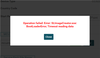
      We have designed a custom board by using CC3220S chip. When firmware loading through UART pins it shows the error, "BootLoaderError, Timeout Reading the data". I followed the CC3220S Launchpad design files and CC3220 Prduction Line guide user manual for my design. 

For Firmware loading  pin connections are Lunch Pad XDS110 UART TX connected to CC3220S RX(57), XDS110 RX line to CC3220S TX(55) , XDS Reset Pin to CC3220S nReset(32) and also make ground line common. The SOP0 ,SOP1 and SOP2 settings are Low,Low,High combination used for firmware loading. 

Questions are 

1. Do we need to load any bootloader firmware initially to the chip ?

2. Any issues when Fresh SPI flash chip used?

3. Do i need to use any other PINS (UART TX,RX,nRESET,SOP0,SOP1,SOP2, GND and 3.3V) for programming the chip?

4. Is it possible to verify my Hardware files from your team?

Thank you for your Support in advance.

Abhilash Job

  • Hi,

    Answers to your questions:

    1. No.

    2. There is no issue with blank SPI flash.

    3. Connection of these pins should be enough for proper connection for Uniflash.

    4. You can ask for design review here.

    btw ... How many layers have your board? Can you compare voltage at VDD_DIGx and VDD_ANAx between your board and LaunchPad?

    Jan

  • @Jan D - thank you for answering Abhilash's questions!

    @Abhilash - Also, the SOP settings should be 010 when booting the device to flash the chip via UART. 

    BR,

    Seong

  • Hello Jan,

             Thank you for your Answers,

     Please see my Answers

    How many layers have your board? 

    Ans : 6

    Can you compare voltage at VDD_DIGx and VDD_ANAx between your board and LaunchPad?

    Ans : Custom board Voltage measured ,

             Measured Voltage Between VDD_An1-GND -0.18V,   

             Measured Voltage Between VDD_An2-GND -3.3V, 

            Measured Voltage Between VDD_DIG1-GND -0V,

             Measured Voltage Between VDD_DIG2-GND -0V

    In the Case of LUNCHPAD didn't find these pins to measure voltage.

    Thank You

    Abhilash Job


  • Hi

              Tried SOP settings SOP0,SOP1,SOP2 as 010 and 001, In both the cases same BootLoader error showing.

    Thank You

  • Hi,

    Internal DC-DC of CC3220 is not functional - that means chip does not have proper voltages and from this reason is not running. You should ask TI for review of your design. You should check layout guide as well (especially section 4.2).

    Jan

  • Hi

     Okay Thank you i will send my hardware files for review the design.

    Abhilash 

  • Hi Abhilash,

    I've received the design review request. I will review it and provide feedback soon.

    BR,

    Seong

  • Hi Abhilash,

    I've reviewed your design and emailed back my full report.

    But regarding this specific issue, it is most likely due to the following:

    1. If C6 is 0.1uF, then R2 must be 100k so that the RC time constant meets the requirement to properly boot the device. Note that the device is reset when using Uniflash to program the chip. 
    2. Pin 55 and 57 each require a 100k pull up.

    BR,

    Seong

  • Hi Seong,

              I have changed resistor R2 to 100k and added pull up for Pin 55 and 57, still showing same BootLoader error. 

    See our voltage measured for pins VDD_DIGx and VDD_ANx

      Measured Voltage Between VDD_An1-GND -0.24V,   (Previous it was .18V)  

             Measured Voltage Between VDD_An2-GND -3.3V, 

            Measured Voltage Between VDD_DIG1-GND -0V,

             Measured Voltage Between VDD_DIG2-GND -0V

    Regards

    Abhilash Job

  • Hi Abhilash,

    Here is what I am measuring on those pins:

    1. VDD_ANA1 -> 1.92V
    2. VDD_ANA2 -> 3.28V
    3. VDD_DIG1 -> 1.14V
    4. VDD_DIG2 -> 1.14V

    These measurements were done using a CC3220S-LAUNCHXL.

    It looks like the device may be damaged. Do you have a fresh board that you haven't powered on yet? If you do, try making all of the modifications that I advised (especially removing L4) before powering it on. Then try measuring the ANA and DIG pins again.

    Also ensure that the inductors and capacitors tied to the DC-to-DC pins meet the current/voltage ratings shown in Table 11 of the CC3220 Layout Guidelines appnote

    Lastly, I see the 3v3 voltage rail is supplied from the TPS73533DRBR where the max current output is 500mA. The peak calibration current of the CC3220S when VBAT is 3v3 is 450mA (see Table 8.5 in the datasheet). Depending on what else you are powering on your board from this LDO, 500mA may not be enough. Good EE practice is to double the current capability of what is needed.

    On the CC3220S-LAUNCHXL, we used a TPS62162DSGR, which can supply up to 1A.

    BR,

    Seong

  • Hi Seong,

                   I have tested the Fresh board with new CC3220SF chip and still getting the same bootloader issue. How do i make sure that the chip is damaged on my board?. We received this chip from our Chinese supplier. Could you mention the minimum connection for programming the custom board through CC3220S-LUNCHXL XDS110 and UNIFLASH tool?.

    changed the following on PCB 

    changed resistor R2 to 100k and added pull up for Pin 55 and 57

    From CC3220S-LAUNCHXL the following lines are connected to custom board.

    1. Custom Board TX pin - LAUNCHXL RX Pin (Also tested TX-TX lines)

    2.Custom Board RX Pin -LAUNCHXL TX PIn (Also tested RX-RX connections)

    3.Custom  Board nRESETto LAUNCHXL nRESET pin

    4. Custom Board GND to LAUNCHXL GND.

    5. SOP0,SOP1,SOP2 as 010 

    Please mention the minimum connections required for programming the chip.

    Regards

    Abhilash Job


  • Abhilash,

    Those are the connections required to program the board via UART. 

    I am more concerned about all of the feedback I provided. Here are 4 that I would like to highlight out of the 13 bullet points I shared before. 

    1. Using an LDO that can supply up to 1A or more
    2. Having GND copper pour on all layers
    3. See Section 3.2.2 in the CC3220 Layout Guidelines appnote here and the CC3220S-LAUNCHXL reference design files here. There should be three traces routed on the GND layer under the Top Layer that serve as return current paths for the decoupling caps that are tied to 3 main power pins.
    4. It is recommended to place GND vias under the CC3220 as shown in Section 4.5 in the Layout Guidelines appnote to ensure optimal thermal dissipation.

    I advise that you request a new design review before fabricating a new revision of your board.

    BR,

    Seong

  • Seong,

        Thank you for your time and review, We will design new board and send it for review before fabricating it.

    Thank You

    Abhilash Job

  • Abhilash,

    I will be closing this thread. Please start a new thread for any other queries.

    Thanks,

    Seong

  • Seong,

            I have sent our new design files for hardware review, we have done all above mentioned corrections in the layout and Schematic. Please review the files.

    Thank you

    Abhilash Job

  • Abhilash,

    Yes, I received the design request last Friday. I will review the design files and provide feedback via email within this week.

    Thanks,

    Seong

  • Seong,

             Did you review the design files?

    Thanks 

    Abhilash Job

  • Hey Abhilash,

    I'll provide feedback by tonight.

    Thanks,

    Seong