Hi team,
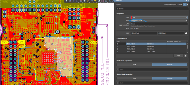
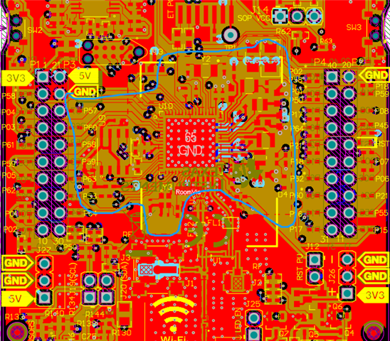
The PCB of the CC3235 Launchpad dose not have copper laying on the part of the blue box in the following figure, why?
Thanks.
Best Regards,
Cherry
Hi team,
The PCB of the CC3235 Launchpad dose not have copper laying on the part of the blue box in the following figure, why?
Thanks.
Best Regards,
Cherry