This thread has been locked.

If you have a related question, please click the "Ask a related question" button in the top right corner. The newly created question will be automatically linked to this question.

LAUNCHCC3235MOD: What do these components on the launchpad do?

Part Number: LAUNCHCC3235MOD
Other Parts Discussed in Thread: OPA4342

Hi,

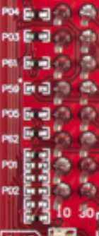
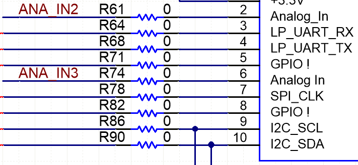
I've been reading through the CC32235MODSFD laundhpad user guide from http://www.ti.com/lit/ug/swru548/swru548.pdf, but I couldn't find an explanation of the highlighted components below. Can anyone provide an explanation of what each of these components do on the launchpad?

  • Hi,

    Please see design files (schematic) for CC3235MOD LaunchPad.

    • U9 - ADC buffer using opamp OPA4342
    • J3 - connector for P01_GPIO_10, P02_GPIO_11, P57_GPIO_02,P55_GPIO_01
    • U8 - unpopulated layout for serial flash MX25R6435FM2IL0
    • Q3 - dual mosfet BSS84DW and Q4 mosfet DN358P for SOP1 and SOP0 (SOP combination for hardware factory reset)

    Jan

  •  Thanks. Could you explain the purpose of this too? Are the diode and resistor meant for a boosterpack or for the CC3235 itself?

    Also what is the point of all these resistors if they have a value of 0 according to the schematic? Why not just make a direct trace?


  • Hi Jack,

    I am little bit confused from your questions, but anyway...

    Reason of all 0 orh resistors is very simple. It allow to you disconnect trace by unsoldering of the resistor. From this reason you don't need scratch a PCB trace for disconnecting. What may not be even possible at four layers board. For example by disconnecting resistor R82 and populating resistor R80 you can move P62_GPIO_07 from P1 to P2 connector.

    Path LP_RESET_OUT is a output pin of RESET signal from LuanchPad. Schottky diode D6 is here to do not allow external device connected to LP_RESET_OUT change state of CC_nRESET. When LP_RESET_OUT is held at low using external device it not affect state of CC_nRESET line.

    Jan