This thread has been locked.

If you have a related question, please click the "Ask a related question" button in the top right corner. The newly created question will be automatically linked to this question.

WL1801MOD: Unable to achieve conducted power output greater than 1.8dBm

Part Number: WL1801MOD
Other Parts Discussed in Thread: WL1801, WL1835,

Hopefully I can provide enough info on my first try with this inquiry...

Petalinux 2018.3 (4.14.0-xilinx)

PHY firmware version: Rev 8.2.0.0.242

Firmware booted (Rev 8.9.0.0.79)

I have derived our configuration from the official ini's on GIT.

Our device is setup in AP mode, and regardless of the configured parameters I have been unable to obtain a conducted power output that exceeds about 1.8dBm.  Measurement is being taken from RF_ANT1

I understand that there are regulatory and compliance considerations, but we're still many dB away from getting close to those.  

I get a very similar result (~0.5 dBm) when I use the calibrator with the following sequences...

ifconfig wlan0 down
calibrator wlan0 plt power_mode on
calibrator wlan0 wl18xx_plt stop_tx
calibrator wlan0 wl18xx_plt tx_tone_stop
calibrator wlan0 wl18xx_plt tune_channel 8 0 0
calibrator wlan0 wl18xx_plt set_tx_power 20000 0 0 8 0 0 0 1 0 0 0 0

(11b continuous test) calibrator wlan0 wl18xx_plt start_tx 500 3 500 0 0 1 0 0 00:11:22:33:44:55 01:02:03:04:05:06 0
(11n continuous test) calibrator wlan0 wl18xx_plt start_tx 400 19 3000 0 0 1 0 0 00:11:22:33:44:55 01:02:03:04:05:06 0

The specific area of challenge seems to result from a lack of measurable output change after modifying the ini configuration.

PerChanPwrLimitArr11ABG values are all set to 0xFF

PerChanBoMode11ABG has been left with its default of "40 00 04 70 00 00 00 00 00 00 00 00 18"

Single 2.4G antenna

Now, the main areas I've looked at are the modification of:

PerChanPwrLimitArr11ABG - Whether 2, 7, or 15 dB (0xF) per channel/mode, the output is unaffected (i.e. entire 150 byte array changed from 0x22 to 0xFF to 0x77)

PwrLimitReference11ABG - Changing from 5.0 (0x32) to 25.5 (0xFF) results in a ~8.0 dB output increase

PerSubBandTxTraceLoss - Whether B2 is set to 3, 7, or 10 dB (e.g. where 10 dB = 0x50), the output is unaffected

PerChanBoMode11ABG - When set to either b00 (FW adaptive) or b10 (using MCS7 output power) the result is near comparable.  I can degrade the performance during testing by using fixed BO, but intend to use the defaults

So...  I'm more than a little confused as to why PerChanPwrLimitArr11ABG and PerSubBandTxTraceLoss have no measurable affect on the transmit power - whether in AP mode or continuous tone.

As a result, our real-world performance seems to be suffering and we're at a loss as to how to rectify this.  I was surprised that I couldn't compensate the few dB of insertion loss using the TraceLoss adjustment

I would greatly appreciate any methods to narrow down the cause of this please.

  • Hi Darcy,

    1.8dBm is significantly low. Are you certain that this is not a hardware related issue? Was impedance matching done for 50 ohms?

    How are you measuring the conducted power?

    Also, have you used this wiki page to perform TX testing? 

    BR,

    Seong

  • Hi Seong,

    Is there a way this might still be hardware related if I'm taking the conducted measurement from RF_ANT1?

    Yes, the cables and both the R&S FSL and Sigilent spectrum analysers are 50 ohm.

    The signal from RF_ANT1 is going directly to one of the analysers.

    Yes, I have been using the TX Testing wiki page...  Running the tests is the easy bit.

    I don't understand why the configuration changes aren't having measurable output changes in the way that the documentation claims they should...  

  • Darcy,

    Hardware related meaning, was the PCB impedance controlled? 

    Also, how are you measuring the signal? If you haven't already, use the SA's RMS detector and integrate the channel power over the total bandwidth. 

    Could you please share a capture of the spectrum analyzer measurement?

    Thanks,

    Seong

  • Thanks Seong,

    My WL18xx development kit just turned up yesterday and i've recently got that going...  So now I have a control to compare our device against.

    Yes, the PCB is impedance controlled, designed by our RF engineer.

    I have the SA set up in max hold, with an RBW of 1 MHz and VBW of 3MHz.

    Over the next day or so I'll attempt to migrate our ini/config over to that which I'm using with the development kit.  When I get a bit further, I'll provide a trace using RMS/integration as you've suggested.

    Is there a way in which to export the ini/config from RTTT so that I can use it in our system?  Or something along those lines...  

    Thanks

    Darcy

  • Okay, just as a quick follow-up... 

    Using the same limits INI file and the same firmware...

    When I run the Continuous TX test using RTTT (and the WL1835 dev board), with what I believe are otherwise the same configuration values, I see around 11-12 dBm at ANT1.  Using the same limits file on our WL1801 I see around 0-1 dBm...  

    The carrier feedthrough using RTTT results in slightly lower power outputs than continuous TX, but still at least 6 dBm higher than the WL1801.  And since the question will be asked, I've tested this on three different 1801's just in case it was device specific.

    Aside from the WL1801 vs WL1835 I'm rather at a loss to determine why there is reduced power on the WL1801?

    Question:  Using RTTT, How do I run the equivalent test (0)11b?  I'm unsure how to set that up, and that would provide a more accurate like for like output

  • Hi Darcy,

    In your INI file, try setting the NumberofAssembledAnt2_4 to "1" and NumberofAssembledAnt5 to "0", if you haven't done so already.

    In the RTTT GUI's "Overall Output Power" block, try setting the Antenna drop-down to "Auto".

    If you'd like to change the modulation rate, use the Rate drop-down in the "Packets" block. See the RTTT User's Guide here.

    What are your custom board's CPW-G parameter values?

    BR,

    Seong

  • Hi Seong,

    Our antenna settings are as you've suggested.  I've tried auto, and TX2 for the antenna settings, where auto is what it is presently configured to.  

    I left the modulation rate as it was to match our historic command-line tests that were described further up this thread.

    Using the configuration below, I'm fairly sure this is the equivalent as the below command-lines - or at least as near as possible.  The highest power output I've achieved from the dev board is 11.3dBm (WL1835), and from our board 5.37dBm (WL1801).  We're still unable to get close to the ideal power output.

    calibrator wlan0 wl18xx_plt set_tx_power 20000 0 0 8 0 0 0 1 0 0 0 0
    calibrator wlan0 wl18xx_plt start_tx 500 3 500 0 0 1 0 0 00:11:22:33:44:55 01:02:03:04:05:06 0

  • Hi Seong, Dave (the RF guy :) ) here. To give you a bit of info on our custom board - we've used track/gap/height values to achieve 50 ohms for our FR4 (diel const = 4.4) board using ground-backed CPW using standard calculation methods. The track lengths are minimal and we've tested to ensure we have minimal losses across these at 2.4 GHz. The power levels that Darcy has reported are at the IC output with ~20mm of 50 ohm track (plus 2x 100pF caps) to a 50 ohm UMC connector.

    I notice that the output of the WL1801MOD IC isn't quite 50 ohms at 2.4 GHz (complex impedance = 14-j10, VSWR=~3:1), so I've LC matched this to our board and am confident that we are losing neglible power due to mismatch losses now - the power levels we're reporting seem to be what the chip is transmitting. 

  • Hi David,

    Are you saying that you have two 100pF DC blocking capacitors in series on your RF line? 

    Can you please share pictures of your board and setup that clearly shows how you are measuring the output power from the module? 

    Thanks,

    Seong

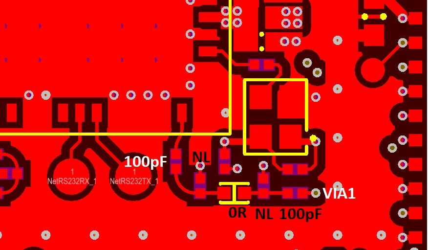
  • Hi Seong, please see screenshots below for our front end tracking.

    The RF output of the WL1801MOD is tracked through series 100pF, 0R, 100pF on the top side of the board. These and some shunt pads are there in case matching is required. The signal passes through VIA1 to the bottom side of the board, where it is fed to our 50ohm UMC connector - this is where we are measuring the TX power in test and AP mode. We connect a 50 ohm UMC cable to our spectrum analyser at this point. 

    The tracks are 0.16mm, gap = 0.35mm, height from ground = 0.08mm, FR4 rel permittivity = 4.2 to give us a G-CPW impedance of ~50 ohms.


    Cheers,

    Dave

  • Bump...  Any further info please?  Is there any evidence of other end-users being able to achieve +10dBm from the WL1801 modules?


    Cheers

    Darcy

  • Darcy,

    Is that a 32Khz crystal that is right above the RF transmission path? Having any type of high speed signal close t to an RF path is not good practice as it could greatly impact RF performance.

    I also do not see any via stitching on the ground plane that you need on both sides of the RF trace. This is mentioned under Section 7.1.3 of the WL1801MOD datasheet. Aside from the via stitching, starting from the 0ohm resistor, a ground plane on the top side of RF path is missing completely. 

    Have you measured the return loss using a network analyzer? With ground plane missing, zero via stitching, and an RF path going through a via without a matching network, is is hard to believe this is matched for 50ohms.  

    I recommend reviewing any of the WL18XXMOD EVM's design files and noting how the RF was designed.

    Some other experiments you can try:

    Have you tried replacing the 100pF series caps with 0ohm resistors? What is the output power with this change?

    Have you tried removing the second 100pF cap and soldering an RF connector to the pad closer to the module and measuring the output power before the via? The same experiment can be done at the first 100pF cap to measure the output power closest to the module's RF pad. 

    BR,

    Seong

  • Thanks Seong,

    I think we're clutching at straws here...  we're going to double check the output strength at the first 100pF location and will then get back with results. 

    Further impedance matching was performed with our network analyser and value tweaks have been made, but that only affected what was downstream rather than measurements taken off this board.

    Please don't close this ticket or marked as solved as I don't believe this to be the cause - but for thoroughness I will check (tomorrow or Friday as we're busy at the moment)

    Cheers

    Darcy

  • Darcy,

    Sure thing. Please also share an image that shows how you soldered an RF connector at the 1st cap location to measure the output power here. Looking forward to the results.

    Thanks,

    Seong

  • Darcy,

    Any updates on this?

    BR,

    Seong

  • Hi Seong,

    Our RF engineer is overseas helping with compliance at the moment, he should be back mid next week.  Thanks

  • Darcy,

    All right, I will leave this thread open. 

    BR,

    Seong

  • Hi Seong,


    With further improvements, we're up to 9.1 dBm.  What should we be able to reasonably expect from this unit?  How close are we to optimal at that power output?

    Thanks

    Darcy

  • Darcy,

    What steps were taken to make these improvements? 

    Please see 5.7 WLAN Performance: 2.4-GHz Transmitter Power in the datasheet.

    BR,

    Seong

  • Hi Seong, I'm curious to know what the real-world expected power output might be please...?

    I believe further tuning between the module and the UNC.

  • Darcy,

    Below is snippet from the WL18MOD FCC certification report. This shows the average conducted power of ch1, 6, and 11 by different modulation rates. Depending on the modulation rate used, the average output power will range from 10~16 dBm. The peak power table is also shown below.

    You can download the WL18xx regulatory certification reports here.

  • Hi Seong,

    Thank you for that.  So it looks as though we're 8-10dB off what we're supposed to be able to achieve.  We're really trying to achieve the maximum range possible with this piece of equipment.  Even using the dev board and RTTT, the best real-world result I've seen is about 11-12 dBm.  How are we supposed to achieve this 17-20dBm please?  There really seems to be something fundamentally missing...


    Thanks

    Darcy

  • Darcy,

    The dev board is what was used for certification testing. Could you please share images of your test set up and spectrum analyzer captures of the measurement? I'd like to see how you are connecting the dev board to the spectrum analyzer and the spectrum analyzer's settings.

    BR,

    Seong

  • Hi Seong,

    I can do this, but we'll probably park this until next week.  I will need to pull the gear out again and set things up.  

    What are the recommended settings for the spectrum analyser?  

    My reply might be as late as mid next week once the product manager is back and we can talk about this in more detail.  We're potentially still 8-10dB shy of where we expected...  so we need to take some real-world measurements and see what things look like.

    Can you please provide a) SpecAn settings, and b) RTTT settings for the 1801 with expected max power outputs (dBm)?

    Thanks

    Darcy

  • Darcy,

    Sure, that sounds good. I am requesting images of the test set up to see what kind of cables you are using to connect your dev board to the PSA. Have the cable losses been taken into account? You also need to consider the loss of the UFl connector, which is usually around a 1dBm loss.

    For the spectrum analyzer settings, set the RBW and VBW to auto. Then set the span low enough (usually around 100~500kHz) and make sure there is a 15+ dBm delta from the signals peak to the floor. This will ensure that your measurements are accurate. Also ensure that the sidebands are included and do an integrated band power measurement.

    The peak and average output power tables I shared previously were from the incorrect cert reports (for WL18MODGI). The correct one is below (for WL18MODGB), but they are similar.

    For RTTT settings, use

    • Continuous TX.
    • Try setting the channel to 6 using 1 Mbps (1 DSSS). The expected avg conducted power measurement is 16dBm +/- 1.5dBm. The tolerance can potentially be observed due to board to board variation.
    • Set the size to 100 bytes.
    • Set the amount of packets to the highest. 
    • Set the delay to the lowest.
    • Overall output power to the highest in dBm.

  • Hi Seong,

    This is perfect!  Thank you.  We'll do this later this week and publish the results back here.

  • Darcy,

    Sounds good!

    BR,

    Seong

  • Darcy,

    I haven't heard from you in a while. I'll be closing this thread. Feel free to open and reply to this thread later or start a new one.

    BR,

    Seong

  • Hi Seong,

    Thanks for all your help.  I don't think we've quite fixed things...  but we're much closer than when we started - lots of incremental changes coming from a variety of locations essentially.  We've clawed back enough that this should be good enough for now  :-)  Thanks again!