This thread has been locked.

If you have a related question, please click the "Ask a related question" button in the top right corner. The newly created question will be automatically linked to this question.

CC3220MOD: Flashing/Connecting Issues with CC3220MODSF newly assembled boards(few)

Part Number: CC3220MOD

Dear Sir/Madam,

Subject: Flashing/Connecting Issues with CC3220MODSF newly assembled boards (for few boards).

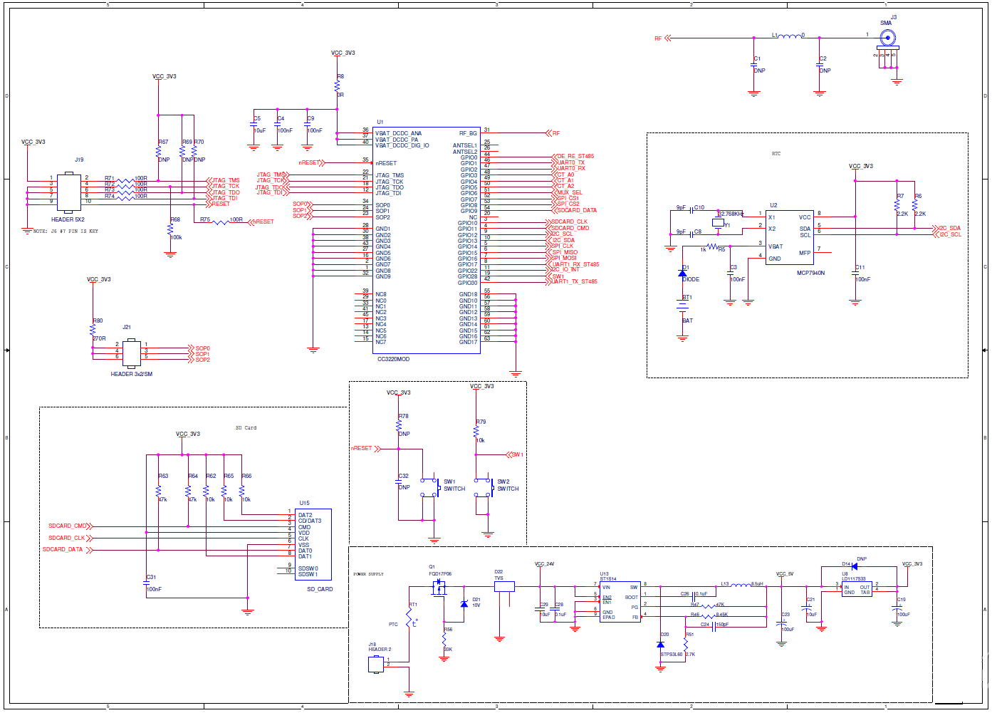
 We are using CC3220MODSF & PFA the Schematic. We are using "CC3220MODASF LaunchPad" for programming(Flashing). We found "connection Fail" issues(Not able to Flash/programming) for Some board(more than 10 boards-Newly assembled) and remaining boards are working fine. We tried to trouble shoot the problem, but everything is looks fine and also we are getting 3.3V from onboard regulator output.

Kindly advise, what is the issues and provide the best solution.


Regards,

Naveen K

  • Hi Naveen,

    It looks like manufacturing issue with your boards. Relatively common with CC32xxMOD is a issue with solder joins under module. Less experienced manufacturing companies commonly have problem with proper paste re-flowof under module. This may to cause short circuits between module pins and malfunction.

    At first step you should to use x-ray or BGA inspection camera and check solder-joints under module.

    Jan

  • Dear Jan,

    Thank you for your reply.

    Can we(Good Manufacturing company) remove the module and re-solder the same module again? It will work?

    How to check whether the module is working or Faulty?

    Is there any CC3220 IC-Jig available to test the module before soldering to the board? 

    Regards,

    Naveen K

  • Hi Naveen,

    Can we(Good Manufacturing company) remove the module and re-solder the same module again? It will work?

    I am not able to answer this question it depends on capabilities of your manufacturing company. But it is generally problem remove module from board and assembly them again. At first step you should too investigate that you have issue with assembling of your module. X-ray inspection is a best way how do this.

    How to check whether the module is working or Faulty?

    In case you have module from reputable source (official distribution) it is unlikely that you will have non functional module. Because modules are individually tested during manufacturing.

    Is there any CC3220 IC-Jig available to test the module before soldering to the board?

    I am not aware about publicly available test jig for contacting CC3220MOD. You need to create this jig by yourself or contact specialised companies at that field.

    Jan

  • Dear Jan,

    Thank you for the information and We will go with X-Ray inspection for this issue.

    We have three more different issues, kindly advise.

    1.In this issue, the board was working fie for few weeks. But now CC3220 Module Vbat and GND pins are shorted. 3.3V Regulator was good(If i disconnect CC3220 VCC jumper) only. I have tested,No issues with the reaming components in the board. Why it happens?What are the reasons for this.

    2. In this issue, the board was working fie for few weeks. But now CC3220 Module Vbat and GND pins are not shorted. 3.3V Regulator was good(If i disconnect CC3220 VCC jumper) only. If i connect 3.3V to CC3220, both Module and regulator will gets heat-up. I have tested,No issues with the reaming components in the board.  Why it happens?What are the reasons for this.

    3. In this issue, the board was working fie for few weeks. But now the module showing I2C bus fault error. SDA pin was working,but SCL pin is not completely going Low(The CLK voltage level(CRO) will be 2.5 and ~3.3V instead of >0.5V and ~3.3V). We have multiplexed SCL pin from GPIO12 to GPIO23. There also same issue. Why the I2C bus fault errors comes? Reasons for failure?Why if one pin fails other multiplexing pins are also fails?

    Regards,

    Naveen K

  • Hi Naveen,

    It is hard to say what can be reason of described issues. According my experience that not properly done re-flow of the soldering paste may to cause weird intermittent issues. In the conjunction that you have non functional new boards, I will suspect assembling issues with this boards as well. Another option can be damage by the ESD, but from information which I have it is unlikely.

    I think your primary goal should be inspect soldering quality of your boards.

    Jan

  • Naveen,

    What is U13 and U8's part number?

    Jan is correct, poor assembly can cause the module to not work properly. For example, if too much solder is used, pin 37 and 38 can get shorted as they are close together, which can cause the module and regulator to heat up. The UART pins 3 and 4 can also get shorted for the same reason, so this may be the reason why you're unable to flash the modules.

    Although from the CC3235MOD datasheet, refer to Section 8.4 PCB Assembly Guide.

    Hope this helps,

    Seong

  • Hi Seong,

    Yes, I had same issue to read schematic. But I think part numbers are:

    Jan

  • Dear Jan and Seong,

    Thanks for the information.

    The Part Number is: U13: ST3485ECDR, U8: LD1117S33TR

    For Led Free(pb-Free) Soldering, Assembly manufacturer(other than previous and one of the reputed assembly company)  said "they required 255 Deg temperature for melting of lead free paste ", but in CC3220 datasheet they have mentioned Peak temperature: 245°C for soldering. So kindly confirm can we go with 255 Degree? Kindly advise regarding this.

    Regards,

    Naveen K

  • Hi Naveen,

    Are you really sure that U13 is a isolated RS-485/RS-422 transceiver? At your schematic at your first question it look like DC-DC from 24V to 5V.

    At chapter 8.5 of datasheet is recommended to use solder paste Sn/3.0 Ag/0.5 Cu. Generally this type of paste have melting point at 220°C not 255°C.

    Jan

  • Dear Jan,

    Sorry for the wrong part. U13 is ST1S14PHR.

    Yes in datasheet it's mentioned, even i shared same page to Assembly manufacturer. They are telling they need 255 Degree for 4 layer board otherwise it may cause un-connectivity or after few days it will act as dry solder. Even they have Tested with Testing-boards and they saying, 245 degree giving unfinished/Dry soldering and 250 to 255 Degree giving Good Soldering.They will keep Max Temperature of 255 Degree in final stage for 20 Seconds.

    Otherwise they are suggesting to go with Leaded Solder it will less than 240 Degree.

    Kindly advise to take a decisions here, If 255 Degree is Ok we will go with Leaded type or else we need to go with Lead type.

    Regards,

    Naveen K

  • Hi Naveen,

    Please wait for answer from TI side.

    BTW ... was you able to find wrong solder joints at your faulty boards?

    Jan

  • Naveen,

    The peak temperature must be updated in the CC3220MOD datasheet. The peak temperature is not 245 degrees C, and should be 260 degrees C.

    BR,

    Seong

  • Dear Seong,

    Thanks for the information. We will very happy If peak Temperature is 260 Degree. This time we have changed the Assembly manufacture to check the quality and performance of the board.We also do X-Ray after assembly.

    But in given link/datasheet its showing 245 Degree only as shown in the image. I could not able to find the updated "260 degree" in the datasheet, Could you provide the Datasheet link or image?

    Regards,

    Naveen K

  • Naveen,

    As mentioned, this section of the datasheet must be updated. It will be updated to what stated in the CC3235MODx datasheet. See page 92.

    BR,

    Seong

  • Dear Seong,

    Thanks for the information and we will consider all these thing(Assembly Quality, X-Ray, ESD) for assembly for the new boards.

    Regarding to the Faulty board, we will do X-Ray and check the assembly quality.We can found 2 cases. But my question is:

    1. Case 1: Assembly was not good, Soldering Joint Issue: 

    In this case,re-assemble the module and can we use same module for assembly or have to use new module?

    How to check re-assembled module is working or not?

    2. Case 2: Assemly looks good, No soldering Joint issue, No short circuit:

    In this case, what we have to do? can we use same module for assembly or have to use new module?

    3. If isopropyl alcohol went inside the module while cleaning there is no issue right?

    Regards,

    Naveen K

  • Naveen,

    1) As long as the module isn't damaged, you can try assembling it on a board again. There are different ways you can check to see if the module is functioning properly. A quick bring up would be to try programming the module with an example from the SDK and validating that it works as expected.

    2) I would try to debug what the issue is first before jumping to any conclusions.

    3) Yes, just ensure that it is dry before doing anything else. After using flux remover on my boards, I always blow compressed air onto the board and inside the module to quickly dry the flux remover off. 

    BR,

    Seong

  • Dear Seong,

    Well noted,Thank you for the information and appreciate your support.

    Is there any method to test the re-assembled module without assembling(soldering) on the board? Is there any Testing Jig available like IC Socket?

    Because if the module is not working we need to re-assemble it again and many time re-assembling may damage to the PCB Pads. Kindly advise.

    Regards,

    Naveen K

  • Naveen,

    I understand the issue, but unfortunately, we do not have a jig that can be used to test modules by itself. You will need to create your own solution. 

    BR,

    Seong


  • Dear Seong,

    Thanks for the information.

    Could you please verify the Layout design of CC3220 and more importantly the Antenna Part.

    Regards,

    Naveen K

  • Naveen,

    Please see my comments below:

    1) Ensure the copper cut out on the top layer under pin31 is as shown in Figure 7-3 of the datasheet.

    2) I see that you are using "relief connect" as opposed to "direct connect". I recommend you use "direct connect" so that your GND pour directly connects to the GND pads of the module.

    3) The PCB area with the circuit tied to pins 34~40 are fairly close to the RF transmission line, which is not recommended as it could affect the RF performance. See the MODx reference design Figure 1-21 in the LAUNCHCC220MODASF User's Guide and note how this section was laid out on the other side of the CC3220MODx, away from the RF circuit. You can also download this CC3220MODx reference design here.

    4) Ensure that your transmission line is 50 ohms by having the appropriate CPWG parameters (stack-up, trace width, gap distance, dielectric constant). 

    5) Place more GND vias in the areas shown with yellow boxes in the image below.

  • Dear Seong,

    Thanks for the information.

    1. As per the LAUNCHCC220MODASF User's Guide  “Figure 1-24. CC3220MODx Bottom Layer” under the pin 31, there is no cut out in all 3 layer (Inner layer’s and Bottom Layer) and there is a ground pour in all the layers under pin31. We have referred this figure only. But in Figure 7-3 of the datasheet, it showing only top Layer. So we thought, we can use Ground pour layers under the pin31. Can we use or we need to keep out copper cut out under pin31? Kindly re-confirm.
    2. Noted.
    3. Noted.
    4. We have designed(Trace Width, Spacing, Layer4,FR4) as mentioned in “Table 1-16. Recommended PCB Values for 4-Layer” in the LAUNCHCC220MODASF User's Guide, we have not doing impedance matching in the PCB Fabrication. Is this OK or we need to Match the impedance in PCB fabrication too?
    5. Noted. Also advise Presently the design having the vias. Kindly advise its required this much Density(Number) of the vias or we need to reduce the number of vias?

    Regards,

    Naveen K

  • Naveen,

    1. Leave the GND pours on the other 3 layers under pin31. The purpose of pointing you to Figure 7-3 was for you to ensure that there is the 45.373mil, 14.2mil, and 10.8mil clearances from the RF pin.

    4. Once you have your PCB fabricated, I would measure the return loss and do impedance matching as needed.

    5. Please refer to the CC3220MODx reference design files that I linked in my previous post.

    BR,

    Seong

  • Dear Seong,

    Thanks for the information and noted well.

    The new boards are came from assembly and all boards are working fine this time. But for Old boards we need to do X-ray for finding the issues.

    4. How i can measure the return loss? Is there any tool for that? Could we measure or working experience required?

    4. Can we measure the Impedance by normal multimeter? How to do Impedance matching? By choosing Inductor value right?If yes please share the design document.

    Regards,

    Naveen K

  • Hi Naveen,

    If you want properly match your RF path you will need RF equipment like VNA (vector network analyser). This you cannot do by normal multimeter definitely. In case you will need match your antenna inside device case, you will need do measurements inside anechoic chamber.

    Please watch this video about importance of proper antenna design.

    Jan