This thread has been locked.

If you have a related question, please click the "Ask a related question" button in the top right corner. The newly created question will be automatically linked to this question.

CC3220SF-LAUNCHXL: Cc3220sf & Fatal: CS_DAP: Error connecting to the target: (Error -1170 @ 0x0) unable to access the DAP.

Part Number: CC3220SF-LAUNCHXL
Other Parts Discussed in Thread: CC3220SF, ENERGIA, UNIFLASH

Hi,

I was using my cc3220sf and it was working fine but when I changed a few wires connected to the board while it was working and tried to upload the code (using energia), it gave me this error:

Fatal: CS_DAP: Error connecting to the target: (Error -1170 @ 0x0) unable to access the DAP.


Ps1. I have another program on sFlash and when I pluged the usb I didn't wait for that to start working and I just uploaded the new code.


Ps2. I didn't change the sop configuration and it's still 010. The device manager can see Both XDS110 class application UART and auxiliary Data port.

I tried to reset the board this ways:

1. Put SOP as 000. Unplug the usb. Press switch 1 and while holding it, plug the usb back. 

2. Put SOP as 000. Unplug the usb. Press switch 4 and while holding it, plug the usb back.

Any recommendations would be appreciated. 

P.S.3. I have asked this question in 43oh as well and I was forwarded to this platform. there is an image of my board there: forum.43oh.com/.../

What can I do to fix this?

Thanks 

  • Hi,

    Have you ensured that your CC3220SF is in development mode? If it is not in development mode, the JTAG interface is locked, causing the error you see.

    Please take a look at this SimpleLink Academy module for instructions on how to flash your device to development mode: https://dev.ti.com/tirex/explore/node?node=ABEoqU9o3snoxDcmIpW0EA__fc2e6sr__LATEST

    Regards,
    Michael

  • Michael Reymond said:

    Hi,

    Have you ensured that your CC3220SF is in development mode? If it is not in development mode, the JTAG interface is locked, causing the error you see.

    Please take a look at this SimpleLink Academy module for instructions on how to flash your device to development mode:

    Regards,

    Michael

    Hi Michael.

    Thanks. Yes it was in the development mode and I could connect to it with uniflash as well but now, not only I can't upload a code to it via energia, I can't connect using uniflash as well.

    I could upload code several times that morning but then it just stopped working. It happen when I tried to change some pins and also interrupting the upload. (Starting a new upload before the previous one was done).

    Is it possible to have it switch to another mode automatically?

  • I mean is it possible that it automatically switch to another mode?

  • Hi Michael,

    I ended up buying a new board as I believe I have damaged this one.

    It was in the development mode and I was successfully uploading my code on it so that can not be the problem.

    I believe It hapened because I was playing around with the pins trying to attach my  HC-SR04 sensor to 23-24 or 3-4 instead of 14-15 pin(energia pin naming).

    Any way now I have another question. Why do we have duplicated header pins on CC3220SF launchpad? I have posted the details of my question here:

    That would be so kind of you to take a look at it.

  • Hi,

    Please see schematic for LaunchPad. I think it will explain all. Pin P64_GPIO_09 is connected to pin 9 at P3 via 0ohm R90. But there is no physical connection to pin 4 at P4 due to missing R63 which is not populated. If you want to use pin 4 at P4 you need to populate this R63.

    Reason for this is to allow higher flexibility of connecting pins from CC3220 QFN.

    Jan

  • Thanks Jan, 

    It helped a lot. using a multimeter,  I could see pin 9 at P3 has connection with the left side of R63 (the left tiny dot) but It didn't make sense to me. 

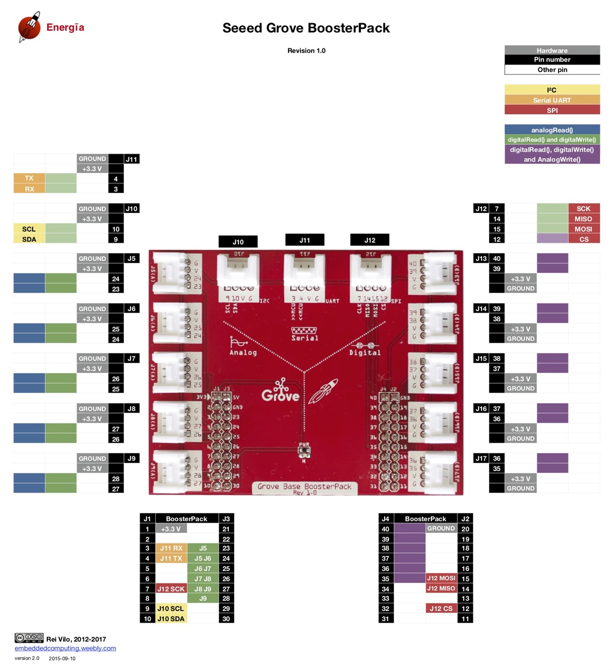
    I am trying to use the GroveBoosterPack (attached is the pinmap) with my board but as can be seen, it doesn't pin out the pin 9 at P3 but it does pin out pin 4 at P4 at J15.

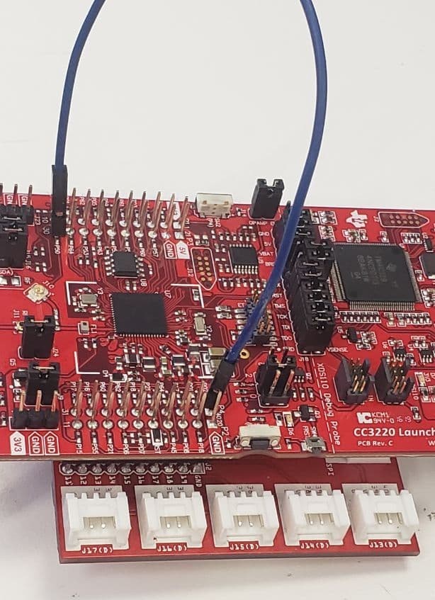
    As I cannot apply any permanent change to the board, I was thinking of just connecting pin 9 at P3 and pin 4 at P4 using a jumper wire instead of populating it.

    That would be great if I can know your opinion on this. [Just trying not to damage this second one :))]

    Regards,

    Negar

  • Hi Negar,

    CC3220SF LaunchPad is designed to capability re-mapping i/o pins to different places of booster pack connector via 0ohm resistors. If you need to change physical connection of pins, there is not much options then using soldering iron. Tinny dots are for DNP 0 ohm resistors.

    Unfortunately I am not familiar with that booster pack and from this reason I cannot give you any advice at this meaner.

    I am not sure what exactly you did with your previous LaunchPad. A few times I saw damaged CC32xx QFN chip by ESD. But generally are CC32xx QFN chip pretty resistant. But do not forgot that i/o pins of CC32xx devices are not TTL (5V) tolerant and pins at ADC mode have even lower maximum voltage than digital pins.

    Jan

  • Thanks for the feedback Jan.

    I believe I did put 5v on either 3 and 4 or 23 and 24 or both sets :). 

    I am thinking of using a jumper wire instead of soldering. when I am checking the connection, pin9 on p3 is now connected to J15 on the grove booster pack but I am a bit worry about turning the board on :))

    also here it says  "you can physically/electrically connect the Grove module to the appropriate pin. " but I'm still searching to see if anyone did this and it was fine or not. no I have to triple check everything. 

    Any way, thanks for your help. I wont push the "this resolved my issue" key because the original issue or the title of this post is sth else. but you did answer my second question and I appreciate it.  

  • Hi Negar,

    Connecting the P64 signal from P3-9 to P4-4 is perfectly fine. The header pin on P4-4 is electrically not connected to anything else, due to the lack of the 0-ohm resistor. In fact, you could safely connect any signal from the board to that header pin if you wanted to. Of course, if you wanted to get the P64 signal out of that header pin, populating that 0-ohm resistor would be all that you need to do.


    Hope that helps answer your question.

    Regards,

    Michael

  • Thanks Michael,

    It definitely makes me more confident to use this connections next time I'm in the lab. I have to use the jumper wires anyway as I need p30 on the booster pack as well :)

    Regards,

    Negar