A related question is a question created from another question. When the related question is created, it will be automatically linked to the original question.
If you have a related question, please click the "Ask a related question" button in the top right corner. The newly created question will be automatically linked to this question.
CC2592: R+jX of the antenna port not listed in the datasheet. What is the impedance?
For the same reasons as listed here: processors.wiki.ti.com/.../CC26xx_Optimal_Load_Impedance the CC2592 does not have a "optimal load impedance" value stated in the datasheet. The recommendation for best RF performance is to follow the reference designs closely.
Can you provide the algorithms to calculate the passives for the matching circuits off your "optimized reference designs" when the stack-up / dielectric are changed? Since you do not provide the R+jX I cannot simply calculate that my self.
I recommend that you use the same dielectric thickness between the RF layer (top) and the ground plane (layer 2). Increasing the thickness slightly is typically fine, but I would not recommend decreasing it due to parasitic capacitance.
If you need to use thin dielectric layers due to micro vias for example, you can place the ground plane on layer 2 or 3 and simply keep the layers in between free for copper in the RF area.
The dielectric constant in the PCB substrate does not influence the matching significantly. We have actually stopped specifying a specific value for our kits, as we do not see any noticeable variation because of it.
With 330 um thickness between the RF layer and the ground plane I think you should be ok. Looking at the schematic here: www.ti.com/.../tidriz6 , the DC block, C27, is your 50 ohm point. You need to match your antenna to 50 ohm here.
Keep in mind the impedance matching and filtering out the chip is not developed through simulations and calculations alone. We have done a significant amount of testing and measurements, especially load- and source -pull, to get the performance right. And it is not only the impedance at 2.4 GHz that matters, impedance at all harmonics is also critical for good performance. Thus the recommendation to follow the reference closely.
It can effect it quite a bit a few ohms depending on how much you care about getting as close to that 1.0 VSWR as possible. Is it tuned with the DC block or before the DC block? If you are this confident that your reference design can be implemented on that stack up, then I will take a leap of faith and use that front end. It scares me to death designing RF blind but we will see how it goes. Since no ammount of testing can prepare you for every situation, that is why having the R+jX measured at the pin is always good to have.
The point is having an impedance number at 2.4 GHz would not make you less blind. You need to hit the right impedance at the harmonics also. To be able to tune the IC match you need access to source- and load-pull equipment.
I have a VNA and a few spectrum analyzers. The problem is the lack of chamber, but you can get away without one. But thanks for the help. Wish me luck.
One other question before I take a leap of faith. If there are any problems relating to RF mismatching. Does TI stand behind their design enough to give engineering support if problems arise?
Got our boards back from the manufacture and there is a weird problem. The boards work perfectly with Smart RF Studio, using the SmartRF05EB. I can fully control my board through that software. The interesting problem is when it comes to programming. I can erase & program but it fails on trying to verify. Do you have any guess on what could be the issue?
Some of our SW Stacks write configuration settings to flash during the first boot. This can happen between the programming and verification step which will make the flash content appear to be incorrect. You can check this by reading back the flash content and compare manually.
We are using cc2530 and just trying to load up the bootloader. 2 out of our 6 boards can flash and verify perfectly. However, every single one of those boards works flawlessly with Smart RF studio. I am really puzzled what can be causing this.
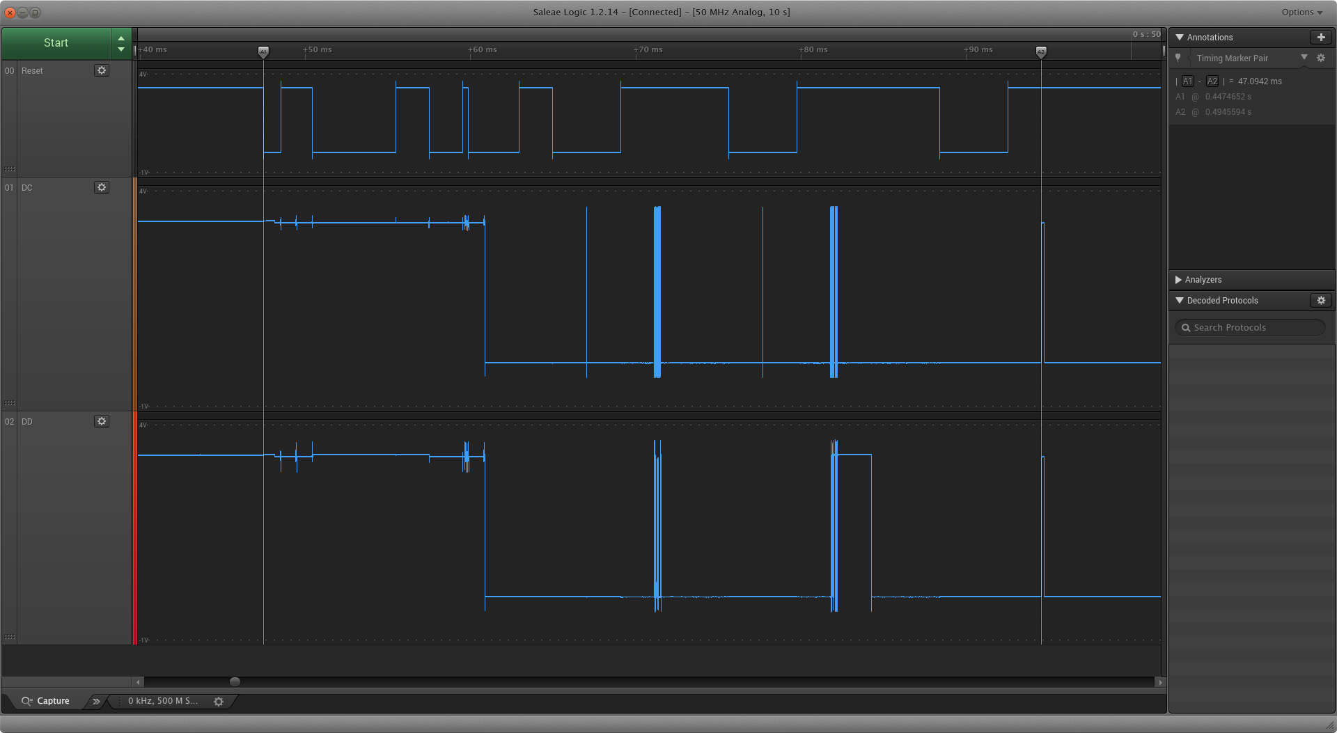
On the ones that work, its pulled low. But on the ones that don't work it's pulled high. I have logic analyzed one of the ones that pull high as it is being plugged to the debugger. It is interesting that it looks like it does not start pulled high but pulls high after. I will attach a few screenshots of the capture.
This is a view of the last "block" of data zoomed in a bit.
Here is the Matlab file (I can do CVS if you have something to read it)
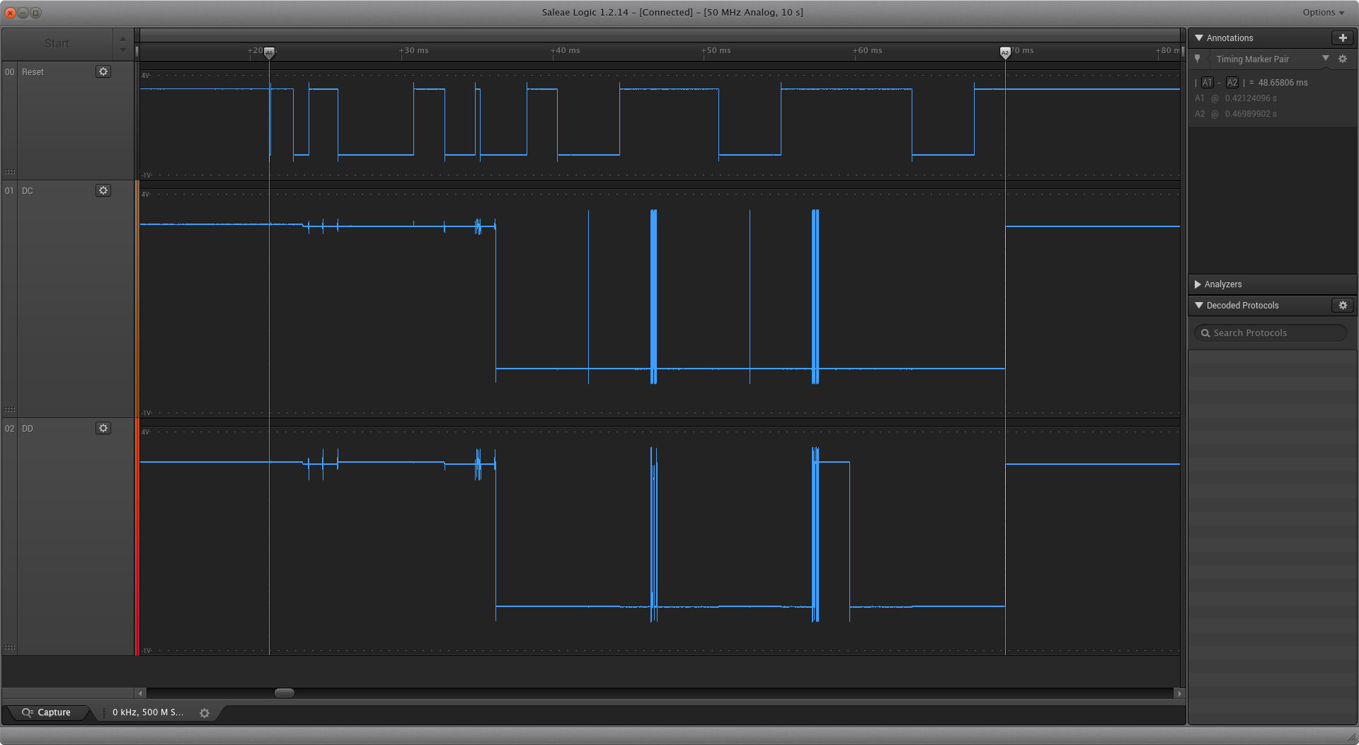
Just did a capture of one working and there is only one difference between the two. I attached screenshots of the two captures. The first one is from a board that cannot be programmed (line never gets pulled back to low) and the seconds one is from one that can (line gets pulled to low)
Hmmm. This is strange. Can you also compare the reset signal? Do you have any pull-ups mounted on the debug lines? Are you able to read the info page on the failing units? What happens if you change the interface speed to slow?
The reset signals look the same, I did notice the reset lines looking like they coupled with the DD line for some reason. However, I busted out an EVM board to compare against and the coupling was there too.
No pull-ups or the debug lines and I am able to read the page on the failing units. The same problem persists in slow mode as well.
Sure thing. The top one is the startup of a working board connected to a cc debugger and the bottom one is from a non-working board. I also attached Matlab data for each capture.
I found the issue out and would like to report if you run VCC to the DCOUPL pin like a derp like I did then you will have these erratic behaviors. I am actually surprised some of them kinda worked 3.6v to a 1.8v pin I figured it would just be fried. Good job making it pretty high tolerances TI.