This thread has been locked.

If you have a related question, please click the "Ask a related question" button in the top right corner. The newly created question will be automatically linked to this question.

CC2652P: Questions about I2C waveforms

Part Number: CC2652P
Other Parts Discussed in Thread: LPSTK-CC1352R

A customer is using CC2652P7 as I2C master with 2 slave devices, and a few questions has been observed when using the I2C example from CC2652's SDK:

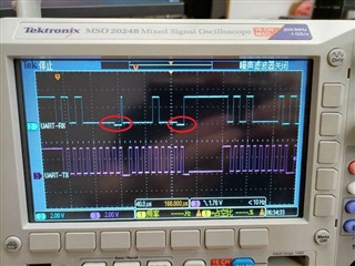
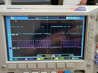
1. SCL was pulled low for a period of time with no good reason, as showed in the purple waveform in below picture. The same slave devices have been tested with other MCUs and no such case was found. Is there a way to tell whether the master or the slaves caused this?

2. A short pulse was found at the 9th SCL clock, see the blue waveform. What could be the cause and how to avoid it?

3. There were small "steps" in the SDA waveform, which appears to be drived by the slave, is it expected behavior?

The customer is using 2.2k ohm external pullup resistors for SDA and SCL pins, and a 33 ohm serial resistor on the SDA/SCL line. Does the resistors have something to do with the issues and what is the recommended values?

Thanks.

Best regards,

Shuyang

  • Hi Shuyang,

    Which SDK are they referencing, are both the master and slave CC2652 devices, and are they using a radio stack concurrently with I2C communication?  

    1. This appears to be clock stretching and is typically caused by the slave if it is not yet ready to process further data.  Or it could be that other processes are being carried out by the master internally before the next byte is prepared to be transmitted/received.  
    2. It could be caused by passing the data line control between the master and slave.  They could try increasing the bit rate to see if this helps, but this is mostly maintained by the TI Driver and overall it should not affect communication since the clock line remains low during this time.
    3. I'm not sure exactly what you mean, could you please clarify?

    You could have the customer try using different pull-up values (the LPSTK-CC1352R uses 3.3 kΩ) or configure internal pull-ups on the pins while not in use to observe how this affects performance.  However, I do not think these will change the behavior your have described.

    Regards,
    Ryan

  • Hi Ryan,

    For question 3, the "small steps" means the logic 0 has 2 different voltage levels, as the below picture:

    And there is one more thing I would like to confirm, does the SDA/SCL pins configured to be open drain in the TI Drivers? Could you help verify this because the driver's source code is in the library.

    Best regards,

    Shuyang

  • The distinction you are pointing out is from the I2C slave pulling down on the data line to indicate a data ACK, you can also observe it from the clock line when a data byte has been transferred and the slave is stretching the clock until it is ready for the next transaction.  This could be caused by a difference in GND between the devices or the series resistor.  The I2C driver initializes the GPIO pins as pulled-up, open-drain outputs.

    Regards,
    Ryan