This thread has been locked.

If you have a related question, please click the "Ask a related question" button in the top right corner. The newly created question will be automatically linked to this question.

CC2640 Antenna

Other Parts Discussed in Thread: CC2640, CC2511

I am doing a project with the CC2640, I know very little about RF design and may need a lot of help. I have decided to use the antenna in AN043 for its small form factor. As I understand it this is a single ended antenna. The reference designs and guides all seem to give different information, making it very difficult to select components. I would like to follow a reference design very closely so as to avoid network analysers and fine tuning etc... A couple meters range will do. Low power is, however, very important.

The CC26xx HW Training shows this option for single ended output with internal bias:
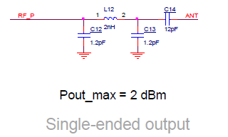
1.) Is this a filter or impedance matching?

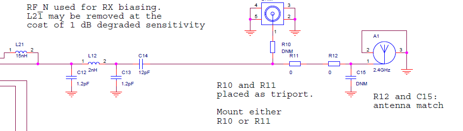
Looking at a reference design for single ended output, I see that there are additional antenna matching components (R12 & C15):
This design does not use the antenna in AN043 but looking at the CC2511 USB dongle which is the reference design for the AN043 antenna, the schematic is even more complicated and does not seem to correspond to the first schematic above at all:
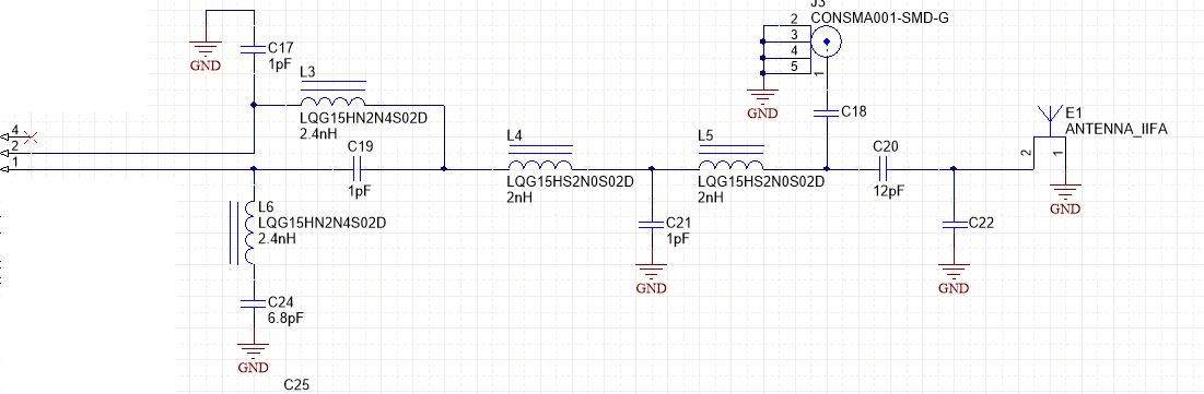
.

2.) What is the most simple way to get this antenna working with the CC2640? My project is mostly about programming, I don't have time to spend on antenna design.

  • Hi,

    Refer to  SimpleLink CC2650 EVM Kit 4XD (CC2650EM-4XD) v1.0.3 Design Files

    Altho it's not the same antenna, the feed point is matched to 50Ohm antenna, means

    that the antenna in current design can be replaced with the one from DN0043.

  • Thanks for the response. The second screenshot from my original post is from that reference design. Can you explain the use of the 0 Ohm resistor R12 and the DNM (do not mount) capacitor C15?
  • These parts are used as placeholders for matching filter.
    Once a PCB produced and the RF parameters are measured, sometimes there's a need (practically always)
    to tune matching between RF path and the antenna.
    If you aren't going to do this kind of tuning, you can leave these placeholders as is, or remove R10, R11, R12, C15,
    making the left pad of R10 your new feeding point. By the way, the track from RF path to SMA connector may
    be omitted too.

  • Thanks, that helps a lot. The problem is, I am not sure if tuning will be necessary. If there is a chance the antenna won't work without this tuning I would like to be sure I have the option to add the matching components. Would a solder bridge work in place of the 0 ohm resistor?
  • It is easier, safer and cheaper to place a footprint for 0R resistor rather than solder bridge.
    If everything done correctly, this design of yours dhould be working OK, not in an optimal way, but OK.
    For people who don't understand a thing in RF matching (like me) reference designs are a MUST,
    and of course a bit of luck.

  • Okay will stick with that then. What about trace width and length? Are there calculations to be done for that? Do I just wing it and hope for the best?

  • Cameron Paans said:
    What about trace width and length?

    Sticking to the track width as in reference design will be a good practice.

    The length can be decreased/increased a little (10mils), however, I strongly recommend

    to keep the same length of tracks between discrete parts in the area between RF_P/RF_N

    pins and the feeding point.

    It is also important to keep the same substrate thickness between the layer with Antenna and the SoC,

    and the first ground layer. For example for a 4 layer design there will be layer1, layer2, layer3 and layer4

    (L1, L2, L3 and L4). Assuming that L1 is the layer with a SoC and Antenna, L2 must be covered with solid

    ground plane (as in reference design) and the substrate thickness between L1 and L2 must be kept as

    in reference design gerber file. L3 will be used for power distribution and L4 (like L1) used for signals.

    Cameron Paans said:
    Do I just wing it and hope for the best?

    Didn't I mention something about a bit of luck? :)

    Well, we are engineers after all, so luck is not our best friend (a "worst case scenario" is),

    therefore you always can post your final schematic and PCB design here in forums for others

    (including RF engineers from TI) to review and get you tips and pointers.

  • Will be sure to run the design through the forum before I go ahead. Thanks again for the help, hopefully luck is on my side. :)