This thread has been locked.

If you have a related question, please click the "Ask a related question" button in the top right corner. The newly created question will be automatically linked to this question.

Programing CC2640 with DevPack

Other Parts Discussed in Thread: CC2640, SN74LVC1T45, TXS0108E

Hello,

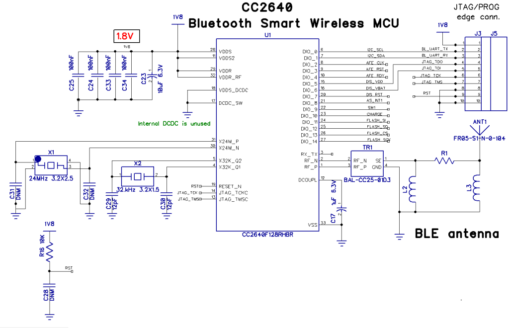
I'm trying to program a CC2640 (7x7) with an DevPack debugger. I'm using the devpack alone without the sensorTag. 

I've connected the devpack to my PCB using the 4-wire JTAG interface: TMSC, TCKC, TDIO and TDO. Also, I've also tested with the nRESET.

I think the Devpack is working because I've obtained this output with the  xdsdfu tool:

USB Device Firmware Upgrade Utility
Copyright (c) 2008-2015 Texas Instruments Incorporated. All rights reserved.

Scanning USB buses for supported XDS110 devices...


<<<< Device 0 >>>>

VID: 0x0451 PID: 0xbef3
Device Name: XDS110 with CMSIS-DAP
Version: 2.2.4.2
Manufacturer: Texas Instruments
Serial Num: 00000000
Mode: Runtime

Found 1 device.

However, when I tried to program a project with the CCS I always obtain the same error:

Error connecting to the target:
(Error -2131 @ 0x0)
Unable to access device register. Reset the device, and retry the operation. If error persists, confirm configuration, power-cycle the board, and/or try more reliable JTAG settings (e.g. lower TCLK).
(Emulation package 6.0.14.0)

The test connection output is:

[Start: Texas Instruments XDS110 USB Debug Probe_0]

Execute the command:

%ccs_base%/common/uscif/dbgjtag -f %boarddatafile% -rv -o -S integrity

[Result]


-----[Print the board config pathname(s)]------------------------------------

C:\Users\jblesa\AppData\Local\TEXASI~1\CCS\
ti\0\0\BrdDat\testBoard.dat

-----[Print the reset-command software log-file]-----------------------------

This utility has selected a 100- or 510-class product.
This utility will load the adapter 'jioxds110.dll'.
The library build date was 'Jul 23 2015'.
The library build time was '19:45:35'.
The library package version is '6.0.14.0'.
The library component version is '35.35.0.0'.
The controller does not use a programmable FPGA.
The controller has a version number of '5' (0x00000005).
The controller has an insertion length of '0' (0x00000000).
This utility will attempt to reset the controller.
This utility has successfully reset the controller.

-----[Print the reset-command hardware log-file]-----------------------------

The scan-path will be reset by toggling the JTAG TRST signal.
The controller is the XDS110 with USB interface.
The link from controller to target is direct (without cable).
The software is configured for XDS110 features.
The controller cannot monitor the value on the EMU[0] pin.
The controller cannot monitor the value on the EMU[1] pin.
The controller cannot control the timing on output pins.
The controller cannot control the timing on input pins.
The scan-path link-delay has been set to exactly '0' (0x0000).

An error occurred while hard opening the controller.

-----[An error has occurred and this utility has aborted]--------------------

This error is generated by TI's USCIF driver or utilities.

The value is '-242' (0xffffff0e).
The title is 'SC_ERR_ROUTER_ACCESS_SUBPATH'.

The explanation is:
A router subpath could not be accessed.
The board configuration file is probably incorrect.

[End: Texas Instruments XDS110 USB Debug Probe_0]

Do you know if it is possible to program a CC2640 with the devpack alone? It is necessary another connection between my board and the devpack?

Best regards,

  • Do you also have common ground and supply to both the board and the debugger?

    .:svend
  • Hello,

    I've already get it. I've just connected the 4-wire JTAG and reset to my board. The GND should be common too. However, the power supply can be independent. In fact, I'm suplying my PCB with an external power source with 3V and it works. 

  • user1472982 said:

    Hello,

    I've already get it. I've just connected the 4-wire JTAG and reset to my board. The GND should be common too. However, the power supply can be independent. In fact, I'm suplying my PCB with an external power source with 3V and it works. 

    Hi,

    Good to hear you have it working. As long as the power supplies are close enough for both devices to correctly detect the logic level a different power supply is OK.

    .:Svend

  • Hi,
    We are facing a quite similar problem... but still not solved :(
    We have built a custom HW, based on the 5x5 chip, and so far no way to program it with the devpack.
    One of the issues may be due the powering of the device which is based on a single 1.8V source (internal DC/DC converter of CC2640 not used).
    We have thus inserted level converters on the different lines between the device and the devpack, but still not successful.
    Apparently TDO does not look similar to what we can observe on the SensorTag, but we still need to go back on the bench to make sure...
    What are the minimum connections for the device to be programmed using the DevPack (we currently use TDI, TDO, TMS, TCK and of course reset)?
    Is there any use of the XDSET_TXD/XDSET_RXD present on J1 connector on DevPack (connected to the so called Skin Connector of SensorTag)?
    We have tried to put a scope probe on it to check the possible handshake during programming of SensorTag, but in that case it failed!
    Thanks for any advice...

    Best Regards
    JYL
  • Do you have a SmartRF06EB as well, as these are meant to be used to program and debug external targets. The DevPack is not made for this, but as you say, with some level shifters, you should be able to make it work. You will need as you say TDI, TDO, TMS, TCK, reset_n and common ground. Have you looked at the documentation for the SmartRF06EB on how the external target is connected to this board and how the level shifting is done on this tool? 

  • Thanks CHS for your prompt reply.

    We don't have a SmartRF06 EB but we had a careful look at it and especially at the CC2650EM-5XD module, which uses the same device as we do.

    We were wondering if TDO and TDI lines were connected correctly (pin 15: DIO5/TDO and pin 16: DIO6/TDI) since SmartRF EB seems to use the cjtag mode using only tmsc and tck. According to the schematic TDI and TDO are not connected to the EM connector 2 (P2): R15 and R16 not mounted.

    Do you confirm the pinout?

    So far, what we can observe, on TDO is each time TDI is pulled down the voltage decreases by a small amount, exactly in the same way as if we were discharging a capacitor through a resistor during the time TDI line is set to 0. This behavior is very strange...

    Do we need to drive TDO with a Pull-up resistor? if so which value would be recommended?

    The level shifting on the SmartRF06 EB module is only intended for the SPI and the LCD, but we use the exact same type of shifters (sn74lvc1t45 that we had on stock).

    We just ordered a XDS100V3 to try to use the 2 wires cjtag mode.
     We should know more about it by tomorrow...

    Meanwhile any advice or comment on the 4 wires standard JTAG mode are welcome.

    Another important point: has someone already used the CC2640 in the external regulator mode: ie single power supply at 1.8V, with VDS_DCDC and DCDC_SW grounded as stated in § 6.1.2.2 of the Technical Reference Manual (swcu117b.pdf). We are still wondering if our troubles are not coming from there...

    Thanks

    JYL

  • As to your last point, yes, we have tested the external regulator mode on these boards www.ti.com/.../cc2650em-4xs-ext-reg-rd, we have an app note on this available very soon. Remember that the internal DCDC must be disabled in SW as well, there are several points on how to do this on the e2e already. So this is not causing the problems.
  • For the 5x5, the TCK is pin 14, TMS is pin 13, TDO is pin 15 (DIO_4) and TDI is pin 16 (DIO5)
  • Many thanks for the clarification.
    Actually, we are not able to do anything by software since we are still not able to program anything to the device... ;-)
    Hope this will change soon!
    JYL
  • You could also check that the current consumption and VDDR/ VDDS voltage are as expected and the voltage at the DCOUPL pin 1.28V to debug further. Where do you connect the level shifters, on a separate board? If the wires between the boards are too long, this can cause issues.
  • Hi Charlotte,
    yes the consumption looks correct and Voltage on DCOUPL pin is exactly 1.27V which should be OK .
    The level shifters are on a separate board, but directly plugged on our main board. The connections are thus very short (about 1 cm).
    Cheers
    JYL
  • Hi,
    Further looking at the schematics of CC2650EM-4XS-Ext_Reg, which is actually very similar to our design, I'm getting confused by the DNM resistors R15 and R16 on TDI and TDO near the level shifters... does it mean that this board is only intended for CJTAG (2 wires JTAG)? In this case, TMS is bidirectional and I would need to change the level shifters I'm using.
    Furthermore, by reading several posts on this forum, we discovered that for example XDS110 was not able of CJTAG, while CC26XX was not able to do SWD... only 4 wires JTAG was this possible with this combination, but I unfortunately am still not able to do it :(((
    Is there a place where we could find this information summarized and be sure of what we are doing without having to make a guess at how it should be?
    Thanks
    JYL
  • I received my XDS100V3 (from Embest).
    Things appear a little clearer since there are ways to change the setting of the JTAG probe in CCS, and it seems to be responsive.
    However it does go much better and I get the error message:

    IcePick_C: Error connecting to the target: (Error -233 @ 0x0) The JTAG IR and DR scan-paths cannot circulate bits, they may be broken. An attempt to scan the JTAG scan-path has failed. The target's JTAG scan-path appears to be broken with a stuck-at-ones or stuck-at-zero fault. (Emulation package 6.0.14.0) =

    A scope probe is connected on both TMS and TCK and none of the lines appears stuck to anything.
    What could be wrong?
    Do we have a problem with the HW assembly?
    What should we check next?

    Thanks
    JYL

  • Also, with the default setting of the XDS100V3, the error message is:
    IcePick_C: Error connecting to the target: (Error -275 @ 0x0) The attempt to poll a target device exceeded its timeout limit. The utility or debugger has requested that a target device be repeatedly accessed for a specific data or status value. This has failed because the built-in limit for the maximum number of attempts when polling the JTAG scan-path has been exceeded. (Emulation package 6.0.14.0)
    to get the previous one, it has been necessary to slow down the connection...
    JYL
  • Hi,

    The situation starts to be very critical for us!

    We are still not able to program our device.

    We have played with all possible setting of the XDS110V3 to try to understand, but still nothing concrete.

    The error messages change according to the setting but still no way to program the device.

    Attached is what we get on the scope in the best case. The signal is sync on the EMU0 line, used as a reset line of the target (tRst is not present on 14pin version of the XDS100V3 we got). Yellow curve is TCK, Blue is TMS.

    Any help is really welcome!!!

    In this particular case the error # is -150: One of the FTDI driver functions used during configuration returned a invalid status or an error

    Thanks

    JYL

  • Hi JYL,

    It sounds like your board might have an electrical problem. Could you please measure the following?

    - Voltage on VDDR pins
    - Voltage on all VDDS pins
    - Voltage on DCOUPL pin
    - Current draw of board (preferrably CC26XX only current)

    It would also be good if you could share your schematic.

    From reading your description you don't say that you have connected your board supply to the sense pin of the debugger or whether you have shared ground. This is needed for level shifting between debugger and board.

    .:Svend
  • Hi Svend,

    Voltage on VDDE abd VDDS is 1.8V (as stated above, using external regulator mode)

    Voltage on DCOUPL is 1.27V

    Current consumption, for the whole board, is approx 9 mA (if CC26XX consumption appears to be an essential measurement, we could mount a board with only power, Xtal  and CC2640 assembled).

    The sense pin has been connected to make sure the debugger will be set in 1.8V to prevent destroying the CC2640. The ground is also connected at all 4 positions of the 14 pin debugger connector. EMU0 is used to generate the reset line (not sure this is the best way to do that, but the documentation is quite confusing on that point).

    Thanks

    JYL

  • Note: Since you have shorted the DC/DC output DCDC_SW, make sure to modify the DC/DC settings in software before flashing the board to disable the DC/DC. This is done in the customer config (CCFG) structure which is included as appBLE_ccfg.c in all our example projects.
    If you don't do this and successfully flash the device you might end up in a reset loop forever (since the DC/DC output will be shorted).

    Based on the voltages and current draw it seems the device is in bootloader mode where it typically draws 6-7mA w/ DCDC.
    Just to rule out everything regarding the board itself you can try to sync the UART boot loader and verify you get a reply?

    You can write 0x55 0x55 to the UART at e.g. 115200 kBaud and you should see 0x00 0xCC being returned.

    If this is OK I would think your problem is mostly related to level shifting issues or the debugger connection. Probe both sides of the level shifter while trying to program and also measure current while programming with a scope to see that there are not multiple outputs driving the same line (you should typically see current spikes > 5mA if so).

    Regards,
    Svend
  • Many thanks Svend for your prompt reply.
    Thank also you for the note about DC/DC converter, but since we are still not able to access the JTAG the risk is still low... (we just try so far to load the stack, but of course, before loading the apps we'll perform the necessary modifications in the code).

    My colleague successfully connected the serial bootloader and was able with Flash Programmer 2 to read for example the MAC address of the device, meaning that it should be somehow alive. I just want to make sure we have access to the JTAG because in case we forget to activate the backdoor in the CCFG, we can brick the device, with no way to recover it.

    I already probe carefully the debugger lines... I'll further investigate it checking also the current as you suggested.
    BTW, is there any summary about the complete detailed wiring and settings in CCS of the XDS100V3 debugger to be able to access the JTAG?

    Thanks
    Jean-Yves
  • Being still not able to do anything with the debugger I decided to switch to the serial boot loader (which as said earlier cannot be an operational solution, because in case, by accident, we forget to enable the backdoor, the device will brick).

    The behavior is however quite strange!!!

    I was able to connect and send the auto-baud command which was correctly acknowledged by 0x00 0xCC (the device is alive and the PCB not that bad!!!).

    I then tried to send the ping commands (0x20) and got ACK in return (0x00 0xCC) as expected.

    I finally tried to send the COMMAND_GET_CHIP_ID command (0x28) which was also well acknowledged and returned an ID (0x80 0x01 0x90 0x00 not sure if this is the expected value). But next Ping command did not provide any return from the device, unless I send 8 times the Ping command and then got a NACK. This  continued repetitively every 8 commands sent: 7 Ping (or also Get_Status) commands provide nothing and then NACK after the eighth one... until I reset the device...

    Is this behavior normal?

    Did I do something wrong?

    Do I miss something?

    Did I get a very bad quality device?

    Should I replace it by a new one?


    The situation was critical, it starts to be now catastrophic!

    Thanks for any kind of support.

    JYL

  • I made very little progresses on my serial boot-loader, but I still do not understand lots of things...

    For example I discovered that by sending 0x00 bytes on the UART while it is receiving (as an SPI connection would do) and sending a Ping command after each command sent, I was able to get a reply from the device each time.

    However, the reply does not correspond to what is described in TRM!!!

    The first non zero byte is not the length of the packet , but ACK (0xCC)!

    In section 8.2.1 there is an example showing that after an acknowledged packet, the devices which is transmitting data also send a 0x03??? is that a part of the next message? is that a part of the ackowledgement process??? this is really confusing.

    Is there somewhere an up-to-date revision of the TRM? I'm currently reading SWCU117B revised June 2015.

    Help is really really needed!!!!!!!

    Thanks

    JYL

  • Just got SWCU117C!
    However Section 8.2.1 is not more accurate since it still states that the first non zero byte is the length of the packet, while it is actually an ACK.
    What is wrong?
    JYL
  • Got it...
    Just need to send an ACK when receiving data after the ACK (which has to be considered as a part of the command and not the reply)
    JYL
  • Correct, you need to ACK the response from the device. Good that you figured that out.

    So it seems that you have figured out how to use the serial boot loader, but your problem is still the JTAG interface, right?

    You mentioned above that you use EMU0 for reset? Can you explain how? Or did I misread?

    You will need to connect the "system reset" (SRST/nRESET) signal from the XDS100v3 to the reset pin of the device to reset it correctly.

    A short note about TDI/TDO connections on the 5x5 EM (and 4x4 EM): These boards are normally connected to a SmartRF06EB, which uses 2-pin cJTAG as the debug interface. In that case, TDI and TDO are not needed.

    For the moment, the XDS110 does not support the cJTAG protocol, so you would need to use the four pins TMS, TCK, TDI and TDO. In addition, you should also connect the reset signal as described above.
  • This is it: Serial bootloader worked as expected while Jtag still is a problem for us...
    And the point is that if by accident the CCFG doesn't allow bootloader, the board is dead.

    Since our last post we made however slight progresses.
    To firstly answer your question about reset, I read in the ccxml file about XDS100 on CCS that there are options to allow reset by toggling EMU0 and EMU1... not really understanding what it was about, I connected the scope on these two lines, changed the setting in CCS and understood there was possibly a way here to activate the nReset of our board, especially because our XDS100 came out with a 14 pins connector which does not provide the sRST signal!

    We are not using the evaluation modules (EM) but are trying to develop our custom design.
    We first tried to use the XDS110 in 4 wires jTag mode: unsuccessful, thus bought an XDS100V3 still unsuccessful.
    We might have had an issue on the TDO line (too capacitive) and level shifters (not necessary with XDS100 thanks to PD pin, but with the XDS110).
    After correcting these issues, and fighting nights and days with the JTAG, we ended up to discover that, on most of the computer we had, the jtag was not always able to operate correctly, depending on the content of the flash (?????) and possibly the way the USB cable was plugged.

    The very last operational solution we got on our dev computer was to use a (strongly) powered USB hub, connected to an XDS110, feeding the CC2640 through a TXS0108E level shifter, as suggested on the schematics of CC2650EM-4XS-Ext-Reg (although TDO and TDI lines does not seem to be used on that board R15 and R16 flagged Do-Not-Mount).

    Depending on the content of the flash, we sometime have to go back to Smart R4F Flash Programmer to do a mass erase of the Flash before being able to use the JTAG... This is very weird, but at least now we can start to try to program the device.

    To summarize we have tried 5 different computers with different version of Windows, we even tried a 6th one under Linux, because CCS provided an install for Linux, but unfortunately BLE stack seems to only exists as a windows installer... bad luck!
    Out of the 5 computers, only one was able to give, as is, satisfying results in the operation of the jTag. One never wanted to install correctly the XDS drivers (an old XP computer), all other allowed to connect, from time to time, with Smart RF Flash Programmer, but never under CCS. Unless we used the fix mentioned above: boost the USB and mass erase the flash before launching CCS...

    Thank You M for your comment and suggestions.
    BR
    JYL
  • JYL,

    Apart from your experiments with EMO0 and EMU1 for reset, did you ever connect the reset (SRST/nRESET) signal from the debugger to the chip?

    That is an important first step to make things work correctly, and may explain why you need to erase the flash using SmartRF Flash Programmer.

    You may also need a new bootloader on the XDS110 to work well together with the TXS0108E. We know that this combination may not work well, since the XDS110 (running old bootloader) will check the status of TCK after a power-on reset. If this signal is low, the XDS will enter DFU mode.

  • Hi M,

    SRST is not present on the connector of our XDS100V3, so it wasn't connected to anything else tahn the EMU0 line, which was programmed to be used as a reset line in CCS (ccxml file).

    the only (almost stable) solution we got so far, after weeks of investigations, is the one described above: XDS110 with TXS0108E level shifter, TDI,DTO, TMS, TCK and nReset lines connected through it, and a powered USB hub...

    It doesn't seem that XDS enters DFU mode, but sometimes the JTAG connection fails and we have to reset everything, even sometimes to mass erase the flash of the CC2640.

    You spoke about a new bootloader for XDS110... is that available somewhere for download?

    Thanks

    JYL