This thread has been locked.

If you have a related question, please click the "Ask a related question" button in the top right corner. The newly created question will be automatically linked to this question.

CC2640+CC-DEVPACK-DEBUG Problems

Other Parts Discussed in Thread: TPS3705, CC2640, CC2650

I am now under huge pressure to complete a project and have made no progress towards being able to program the chip. I have a custom board with the 7x7mm CC2640 on it. I have also used the TPS3705 to monitor voltage levels and handle reset. When I connected the CC-DEVPACK-DEBUG to the board I was encountered with multiple different errors for example:

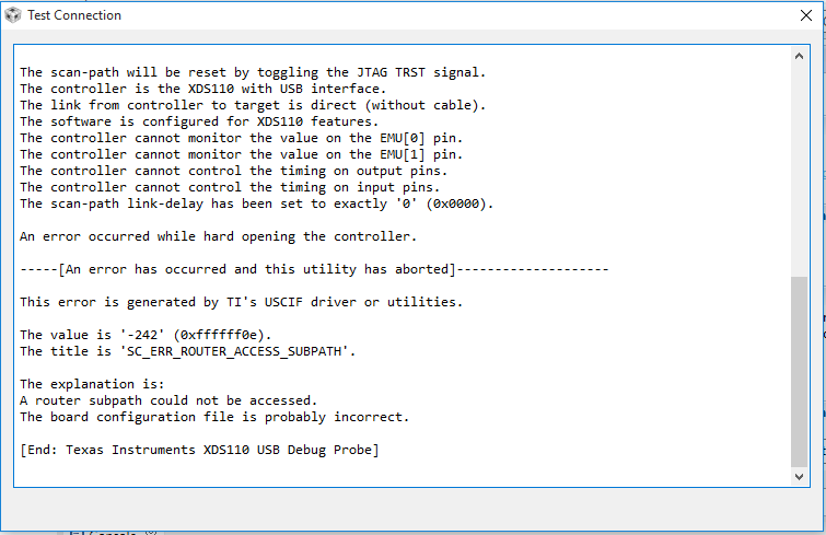
I didn't manage to screenshot them all before the chip died on its own (will get back to that). I have tried the following

  • Windows 10 and 7
  • Latest and older versions of CCS
  • Updated the XDS Emulation Software Package
  • Ran xdsdfu and updated firmware
  • Uninstall and reinstall everything including drivers

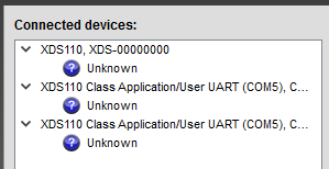
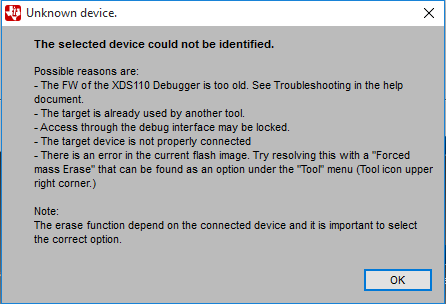
I tried SmartRF Flash Programmer 2, it sees the following:

1) Please suggest where I should go from here.

As I mentioned above, the chip blew. This was after two days of powering up and connecting the debugger.

I soldered on just the basic components and left of all the extras to start with. I used a lab power supply with the current limit at around 0.3A (the current seems to spike this high when powering up). I had the following voltage levels:

VDDS: 3V

VDDR: 1.68V

DECOUPLE: 1.27V

As I understand it, this is correct. The manual reset on the TPS3705 worked no problem as well. The only issue I see being possible is that instead of the resistor and cap on the reset pin, I connected the debugger reset to the manual reset of the TPS3705. 

2) Could this be causing the debugger errors?

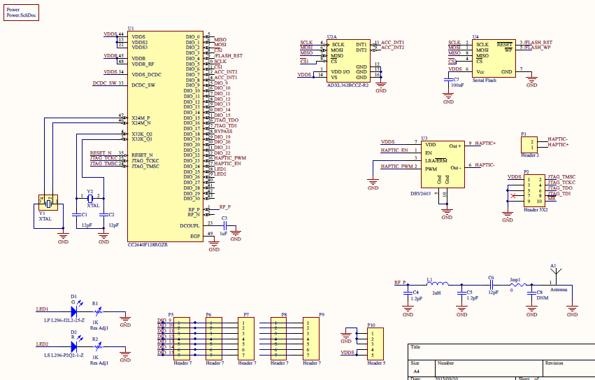
Please have a look at my schematic and layout below:

  • Obviously thats alot of information and I need help fast so I will simplify the question. Lets say I start with a fresh Windows 7 PC and assume I put on a new chip that works. What procedure should I follow to minimise potential problems. Order of installation and specific drivers would be helpful. Thanks.
  • Maybe i am overlooking something obvious, but i cannot see the reset line on the 10pin ARM JTAG header.
  • I connected the JTAG reset to the manual reset of the TPS3705. The manual reset works but i was concerned there would be a delay.
  • Cameron,

    First of all I would test that your PC/driver/SW setup is OK by connecting another device such as the sensorTag to your debugger.

    For debugging you need to connect the reset directly to the CC2640 reset. However it should still be recognized in SmartRF Flash Programmer 2 I think. What is the reason for having the external POR circuit on the board? The CC2650 contains a built-in power-on-reset, brown-out circuit s and a watchdog already.

    Have you also monitored the reset signal from the TPS3705 with a scope to ensure it does not toggle occasionally?

    Regards,
    Svend
  • Hi Svend,

    I really would like to connect a sensor Tag but I am in South Africa and my budget is depleted. I may order one but it wouldn't get here for quite some time.

    As soon as I have a new chip put on I will bypass the TPS3705 for JTAG reset. The board I have designed is essentially an evaluation board. It was recommended that I include a PoR circuit to eliminate problems, I was assured there would be no issues with JTAG in this configuration but I should have consulted the forum first. I mainly included it to monitor VDDR and VDDS levels anyway.

    I have checked it on a scope, no issues.

    Can you think of any reason the chip would have died? It was not connected to the debugger at the time, just 3V. I am concerned that it will continue to happen.
  • The schematic looks correct at least. When you say "chip would have died", does that imply that your setup was working before?
  • No just that the buck converter was working ie. VDDR = 1.68V and DECOUPLE = 1.27V. Now it shorts the power supply.

  • Typical things that would physically damage the chip is ESD damage or externally probing/stopping the 24MHz crystal while both the crystal and the DC/DC is enabled. This could cause the DC/DC to stop switching and charge VDDR up to VDDS.
    A way to find most typical damage is to measure impedance to GND to all VDDR/DCOUPL/VDDS pins when the device is not powered. All measurements should be in the megaohm range.
  • Just did the measurements, all VDDS pins are < 2kOhm. The rest are in the Mohm range. ESD seems unlikely since we have high humidity here but I guess it is possible. I definitely didn't probe the crystal. Could have been a tiny piece of metal on the workbench that caused a short? I hope it is a once off problem.

    What is the maximum current the system should draw while debugging etc? I would like to limit the current more precisely but I definitely had current spikes when powering up, up to around 0.35A. These were not measured but the power supply cut out sporadically on power up if I limited more than that.
  • For the chip itself the highest current drawn will be 20-25mA during bootup (charging VDDR capacitors). On top of that comes all external circuitry.

    Best regards,
    Svend
  • I don't quite understand the statement "manual reset works"? As far as i always thought is that the JTAG XDS programers need to be able to control the reset line for correct timing of debug signals after reset. Your schematic does not show that the reset pin from the CC26xx is connected to the debug header. It's the first thing i would correct. I see you have the reset brought out as a TP so that should be an easy fix.
  • The TPS370 has a Manual Reset pin, i connected the JTAG reset to this. When pulled low it pulls the reset pin on the CC2640 low.  I should not have done it this way as it simply adds another  "moving part". Will be sure to bypass it before trying anything else.  Thanks

  • It was TPS370... It was somehow affecting both the power supply and the debugging. Maybe a faulty chip, not sure. Either way, wasn't a good idea to try connect the debug reset through it.
  • I'm glad you figured it out. It was the only part of your Schematic that looked like a potential culprit. Good luck.
  • Thanks a lot for the help. Now I just have to decipher this RTOS...