This thread has been locked.

If you have a related question, please click the "Ask a related question" button in the top right corner. The newly created question will be automatically linked to this question.

meandered inverted F-Antenna design

Hi,

I have to design a really slim PCB with BLE connectivity and I don't know really much about Antenna design. The only Antennas which can be incorporated spacewise would be a chip antenna or the meandered inverted F-Antenna. After following AN043 I'm not sure if this Antenna can be placed the way shown in the attachment (the drawing is from AB043 and the black area should be the board shape/ground plane.

Is it possible to design it like this?

Thanks & regards,

jl

  • Hi Jogi,

    Yes, it is possible to place the antenna as you have suggested. The ground plane is an important part of a dipole antenna, so the antenna efficiency decreases when the ground plane size is reduced. My guess is however that the performance of your board should be good.

    You can set D2 = D3 = 0 (move the antenna all the way to the edge of the board), and I would increase D1 to 1mm.

    /Fredrik

  • Hi Frederik,

    thanks very much for the very fast and really helpful answer!
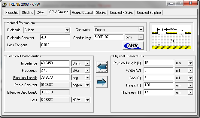
    I want to use a matched balun especially designed for the CC254x devices and a PCB 0.8mm thick. Can you tell me which track/space width I have to use for the antenna connection?

    Thanks again, very much appreciated!

    Rgds,

    jl

  • Hi Jogi,

    Here is a very helpful and free tool to calculate the dimensions of transmission lines: TX Line

    Remember that you really don't need to be too worried about the impedance if your trace length is less than lambda/10. For 2.4 GHz the wavelength (lambda) is approximately 12 cm. However it doesn't hurt to make the impedance 50 ohm even for short traces. :-)

    /Fredrik

  • Hi,

    don't want to mess up my first RF design, so I'd better be careful :)

    Thanks again very much, seems that 9mil track and 7mil space will do the job for me... screenshot ok?

    Rgds,

    jl

  • Looks good!

    Please use the "Verify answer" button so we can keep track on which threads are properly answered.

    /F

  • Hey Fredrik,

    I have some questions regarding the meandered inverted-F antenna;

    We’re working on a new 6 layers board with a 2.4GHz Bluetooth module that requires an external antenna. Due to small space availability on the board we plan on using the meandered inverted-F antenna (using AN043 guidelines).

    1. We plan to have the ground plane on the second layer (with the antenna being placed on the top layer), and have all the antenna's dimensions matching the reference design (the width of dielectric in-between layers 1 & 2 will be the same as ref design) – do you think that would work?

    2. To connect the antenna to the module, we only plan on using a 50 ohms feed line (with no matching or "blun" circuitry) – if you think this is possible, what may be the risks if any?

    3. Also, we currently do not have a network analyzer in-house, what would you recommend to us in terms of design so that we may have the ability to debug and troubleshoot the antenna performance with the first prototypes? What are my options without using the network analyzer? For example, is it possible to extend the antenna length and cut it ourselves (using a sharp blade) to the desired length we need?

    Thanks,

    Asaf 

  • Hi Asaf,

    1. Yes this sounds like a good approach.

    2. If you have room for it I would highly recommend adding a series and a shunt component placeholder (series = 0 ohm resistor, shunt = do not mount) so you have the possibility to tune the antenna impedance if needed. The impedance of the antenna will be affected by factors such as PCB shape and size, plastic housing around the antenna etc.

    3. You can measure the output power level with a spectrum analyzer. To do this you should make some kind of jig to make sure the distance from the PCB antenna to the antenna connected to the spectrum analyzer is constant. Try to cut 0.5 mm at a time and stop when you pass the peak power level.

    Cheers,

    Fredrik

  • Hi Fredrik - thank you for your fast replay!

    I have few more questions though;

    2. Where should we place the series and shunt components? (Does it need to be close to the module radio output pad or closer to the feed line antenna connection?) What’s the shunt for and how do we use it?

    3. What if we don't have a spectrum analyzer? What else can we do to evaluate antenna's performance?

    Thanks again,

    Asaf

  • Hi Asaf,

    2) They should be place as close to the antenna as possible. Both the series and shunt components are for the possibility that you need to shift the antenna impedance. Have a look at this app-note for more details: http://www.ti.com/litv/pdf/swra161b

    3) A spectrum analyzer is essential when developing RF products, so depending on your needs I would highly recommend buying or renting one.

    Cheers,

    Fredrik

  • Asaf,

    If you do not have the RF expertise and need to use CC254x device. You can always use a certified module using CC254x chips with a built in antenna. This way you would reduce the complexity of the RF design for you and focus more on the other aspects of the board. The different TI module partners are given below. Be careful while choosing the modules, make sure they have antennas built in.

    http://processors.wiki.ti.com/index.php/Category:BluetoothLE#TI_BLE_Module_Partners

  • Chatto,

    We are only using the meandered inverted-F antenna, we were looking on some TI BLE module partners but ended up going for the SPBT2532C2 (STMicroelectronics) which was the best solution for us cost and size wise.


    Thanks,

    Asaf