This thread has been locked.

If you have a related question, please click the "Ask a related question" button in the top right corner. The newly created question will be automatically linked to this question.

CC1350: Error -242 when trying to programm CC1350

Part Number: CC1350
Other Parts Discussed in Thread: TPS62740, CC1310

Hi

I want to use a CC1350 on a custom PCB. Since I need a 1.8V power source for other components I use a TPS62740 to generate board wide 1.8V.
To save power I want to use this voltage directly for the CC1350. So I designed the PCB with the CC1350 in External Regulator Mode like describes here (www.ti.com/.../swra498.pdf) and in the technical reference manual to disable the integrated DCDC.
All Vdd pins are connected to the 1.8V output of the TPS62740 except VDDS_DCDC which is (together with DCDC_SW) tied to ground.
In addition I connected a 24MHz and 32kHz crystal.
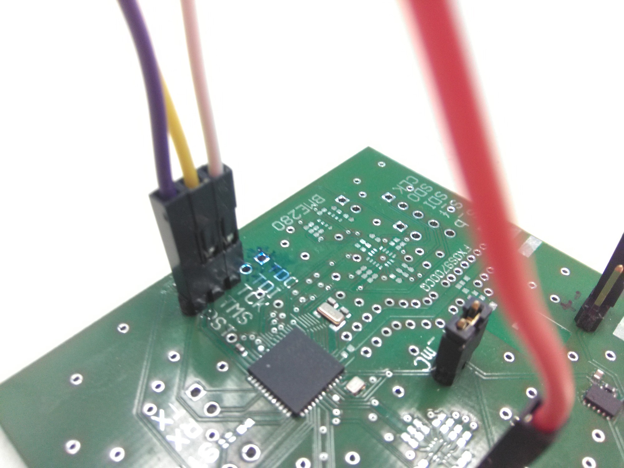
For programming I connected the TSMC, TCKC and RESET pin to the equivalent pins on the XDS110 of a CC1350 Launchpad. RESET has a 100k pull up resistor to 1.8V. The signals from the Launchpad are changed to 1.8V via a level shifter
Thermal pad is grounded. All other pins are unconnected and floating.

Unfortunately with this setup access to the CC1350 via smartRF studio and CCS is not possible.
I either get the error message "Device access failed: XBAL: Target connect failed" (smartRF) or "Error -242 @ 0x0, A router subpath could not be accessed." (CCS).

Does anyone know how to fix this issue?

  • Try to refer to processors.wiki.ti.com/.../CC26xx_HW_Troubleshooting to trouble shooting your CC1310 HW first.
  • Thanks for the link.

    I went through that but it didn't help.

    TCK/TMS/RESET/GND is connected to debugger (Launchpad). Using only these pins I can access the CC1350 on the Launchpad, so debugger itself is ok.

    VDDS* Pins are all connected, voltage everywhere 1.8V. As already mentioned I use the board in external regulator mode with VDDS_DCDC and DCDC_SW connected to GND.

    I have multiple vias on the ground pad and resolderd it to make sure everything is ok there.

    Voltage on DCOUPL is 1.28V and the overall current is around 6mA.

    Only two points from that list not working are a) to disable DCDC in software. Doesn't work since I can't even flash a program.  b) Voltage at VDDR is 1.8V not 1.68V. Since it was written in external regulator mode VDDS and VDDR should be connected this shouldn't be a problem, right?

    Pinging the bootloader I get 0xFFFBFF as response. Doesn't seem to me like the 0xCC ACK signal I found in the datasheet. I tried this with baudrates from 300 to 115200. Same behavior everywhere. I always first send 0x5555, then 'CMD_PING' and in the end unplugged the device before the next try. 

    Below the part of the schematic with the CC1350. All DIO* pins are connected to various GPIO devices which are currently not populated on the PCB. So all DIO* pins are floating

  • If you use Flash Programmer 2, can it recognize your CC1350?
  • A question about the xtal: If you have used a 24 MHz xtal, why is it named 32.00?
  • Neither CCS, nor SmartRF, nor FlashProgrammer 2 recognize my CC1350. Error message from Flash Programmer is: Create XBAL object failed: Target connect failed Failed to create device object.

    In the schematics I used a device we have in our local component library that has 32MHz. On the PCB I used a 24MHz xtal from the same series with the same footprint. So this is just a typo I forgot to fix in the schematic. Sorry for the confusion.
  • Which version of SmartRF Studio do you use? Have you selected 2 pin JTAG in Flash Programmer 2? How is the 1.8 V connected to the level shifters on the LP?

    Do your board and the LP share ground? If not I would assume that the voltage levels are not referenced and the levels could be wrong.
  • I use SmartRF Studio 2.5.1 (build #4). The internal update routine says it is the newest version.
    Yes, in Flash Programmer 2 "Use 2-pin cJTAG" is ticked.

    As level shifter I use a NXP NTS0104. There the Launchpad supplies the 3.3V and my PCB the 1.8V. The push pull level shifter then translates the signals in both directions. I also tried a series resistor as voltage divider with the CC1350 internal logic. I tried each with a different CC1350 in case it gets damaged. Both ways are not working
    In addition to the JTAG signals I also connected the ground of the Launchpad and my PCB.
  • When you said "Yes, in Flash Programmer 2 "Use 2-pin cJTAG" is ticked.", do you mean you can use Flash Programmer 2 to program your CC1350 without problem?
  • no, unfortunately doesn't work there either. That just was answering TER's question if I have that option selected. But even with that option selected I can't access my CC1350 at all. Not with CCS, not with SmartRF and not with Flash Programmer 2
  • It seems 8Q-32.000MEV-T is a 32M crystal. You should use a 24M crystal instead of 32M.

  • Sorry about that confusion. TER mentioned the same thing earlier. This is just a typo in the schmeatic. We had the 32MHz version in our component library so I used that and forgot to change the name. On my PCB I soldered a 24MHz with same footprint from the same series. 

  • From your description I can't see why it shouldn't work. Is it possible for you to take some pictures clearly showing how you have connected your PCB and the LP together? 

  • I hope the pictures are clear enough.

    On my PCB I have connected TCK; TMS; RST
    TMS is connected to the pin 24, TCK to pin 25 and RST to pin 35.
    Other than that I only have the 24MHz xtal at pin 46 and 47 and the 32kHz xtal at pin 4 and 5.

    To make the 3.3V from the LP compatible I used a level shifter for TMS and TCK. RST is directly connected.
    If I check the signals on either side of the level shifter (on the LP and my PCB) they are the same, just have different voltage.
    So the levelshifter itself should work ok.

  • If you don't mount jumpers on 3.3V and GND, I don't think LaunchPad will pass 3.3V to your board. By the way, please remove level shifter between your CC1350 and LaunchPad.
  • Why do you use an external level shifter board? The level shifters on the XDS part of the LP should work down to 1.8 V.

    To me it looks like a voltage level issue but it's a bit difficult to determine exactly what without the hardware in front of me.
  • Apparently something went wrong on my side with the integrated level shifters on the LP.

    I tried it with them the first time. Since it didn't work I switched to external ones. Also failed.

    Now I tried again witht the internal ones of the LP and now I get a connection. I don't know what exactly went wrong the first time and then sent me on this adventure, but now everything is working.

    Thank you to you two for your help and patience.

  • You are welcome and it's good to know it works now.