This thread has been locked.

If you have a related question, please click the "Ask a related question" button in the top right corner. The newly created question will be automatically linked to this question.

CC1350: CC1350

Part Number: CC1350


Hi everyone,

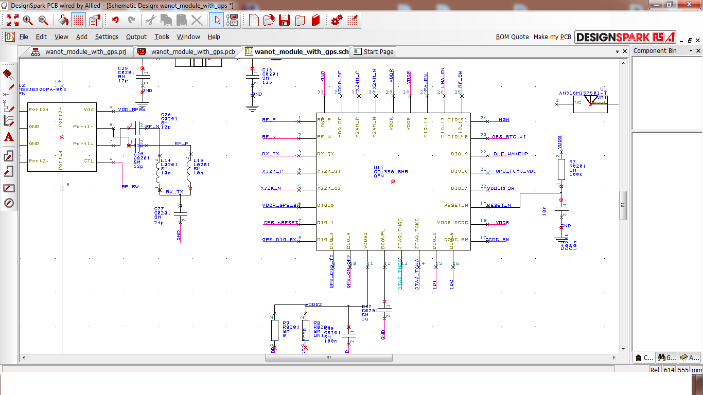
We are trying to jump from CC1350 Launchpad to our custom board and burn the BLE stack. When we do it through the Launchpad we could detect the BLE advertising.

However, when we redirected the same TCK, TMS, Reset, 3v3 and GND pins to our board and burn, Code Composer reaches the same reset state at the end but unfortunately we could not get the BLE radio up

on our board. The only difference between our board and the eval board is the package; we have 5mm RHB while the chip on eval board is 7mm RGZ. Would anyone guess what might have gone wrong?

They have the same amount of flash 128KB. Do we have to do anything specific on the Code Composer Studio while burning to an external 1350 chip?

Thanks ahead

Ahmet


  • I suggest you to use SmartRF Studio 7 to test RF TX/RX to see if it works first.
  • - Why are you running the full BLE stack on CC1350?
    - Have you checked that the correct IOs are used for the JTAG interface and for other external signals you may use?
  • Thanks much YK,

    Yes, that fortunately helped a lot, because I could see the XO and RF activated, now but, our original intention was to burn the BLE stack to be able to get OAD working for fast firmware development.

    However, through RF Studio we could see the XO at least waking up and also it confirmed the communication from our board through 2-pin JTAG. Any idea on how to burn the BLE stack? our target is to achieve OAD (over the air download) through BLE.

    Thanks again,

    Ahmet

  • Hi Guru, We wanted to get OAD working to be able to program it easier. On our unit there was not space for a connector to burn, we went directly to final board, so just two jtag solder pins and reset for burning but everytime resoldering for a firmware fix is too tough. So, we are just looking into an initial BLE code to enable OAD. As an answer to your question, when we tried through smartRF studio, it was able to communicate with our small beacon through these pins and we can control the radio, but not sure why we could not load BLE stack for OAD.
  • Have you tried to flash the device with the carrierwave example to see if it's the JTAG interface or the BLE stack that is the issue?
  • Actually I was also suspicious of the JTAG interface but later when we tried RF studio, it seemed to detect and pass the packets to the radio on our custom board. I am not sure but the problem seems to be related to burning into 5mmx5mm chip through the launch-pad; which carries 7mmx7mm package of the same 1350 chip. So, still trying to solve the issue ! non many seem to be building custom boards with this chip:(

    Best

  • I assume you have changed the board file to reflex that you use a 5x5 and not 7x7?

    I can take a quick look at your schematic if you want (you can send me a friend request and send it that way)
  • Hi TER, this is great clue; I was curious how to refer to 5mmx5mm package in the CCS. Can you please guide us in that, we have been looking at the menus in CCS to see if we could pick such a setup but no luck.

    Also I am attaching the snapshot of the schematic here, everything is quite matched with the TI eval board BOM, as you see though in the schematic we are using only routing out JTAG pins and nreset without TDI and TDO. But the JTAG interface seemed fine while connecting with RFStudio, so the problem of loading the BLE stack should be specifying the 5mmx5mm option based on your feedback, but we could not locate that menu in CCS.

  • Hi Guru,

    Thanks for this, I went through the link as well. Even before hand I just checked the BLE radio itself on our custom board through RF Studio and made sure on the spectrum analayzer that we had the signal in the corresponding channels. Being able to control the channels and observe the output spectrum, we could tell that the 2-pin jtag interface was fine to control the internal registers.

     After this point, we can most probably conclude that it was related to burning the ble stack to a custom board in CCS debugger. When I went through the burn process and modified the files accordingly I noticed that the

    IOs etc all assumed 30 IO 7mmx7mm RGZ package, our costom board though has 5mmx5mm RHB package. How could we differentiate during burn-in? is there any parameter that needed to be set to let the ble stack burned properly? Any help is appreciated! 

  • You basically have to modify the board files to reflect the 5x5/ your pinout as described in the link I posted in my last reply.