Other Parts Discussed in Thread: XTR117, XTR116, DAC8551, XTR111
Hi,

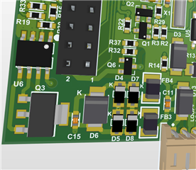
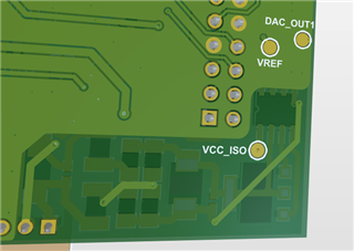

This thread has been locked.
If you have a related question, please click the "Ask a related question" button in the top right corner. The newly created question will be automatically linked to this question.
Hi,


Hi Darshan,
The issue is that 4-20mA current output value is drifted from 4mA to 6mA on the 0 value pressure. We have checked input voltage is same but output current is drifted by default.
Under what CS condition (frequency range) that the current loop is drifting under test. Below is the reference tested under IEC 61000-4-6 in XTR117, which is similar to XTR115/XTR116 2-wire transmitter.

Please check out the markings below. Place series of low ESR bypass capacitors across Vsup if the circuit failed CS tests.
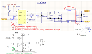
If you have additional questions, please let us know.
Best,
Raymond
Hi Darshan,
They both should pass CS compliance test in IEC 61000-4-6, though XTR117 is the later revision product.
Let us fix the typos in the design and see how XTR115 should withstand the CS test. Also, please add series low ESR ceramic capacitors at Vbus or Vloop to decouple the possible CS interference.
As it is configured, the 4-20mA current loop is not functional. Enclosed is a simulation in XTR115. Please make sure that the DUT is working before it is being tested in CS.

Best,
Raymond
Hi Raymond,
MCU is operated on +3.3V. So we can not use Vreg +5V supply.
We have one question. What is use of R7-250ohm in simulation circuit?
Actually we have check Pin#3 Iret connected with GND. That is not float in any eval board.
Have you any idea regarding IC damage during CS test?
Thanks
Darshan
Hi Darshan,
MCU is operated on +3.3V. So we can not use Vreg +5V supply.
Oops! Then we need to see the full schematic.
Kai
Hi Darshan,
MCU is operated on +3.3V. So we can not use Vreg +5V supply.
As Kai suggested, you should present the entire schematic in XTR115. XTR115 has 2.5Vref and 5Vref pins, and it does not provide 3.3V reference voltage. It is not clear what you have.
Are you doing 4-20mA current loop with 0-3.3V input voltage? From the presented XTR115 schematic, the input resistor values are not quite correct either, even 3.3Vin supply is used.
What is use of R7-250ohm in simulation circuit?
The current loop is from 4-20mA, with 250Ω load, the I-to-V conversion part is from 4mA*250Ω to 20mA*250Ω or 1-5V in the simulation. If you want to convert 4-20mA to voltage in 3.3V full scale, then the resistive load is 3.3V/20mA = 165Ω
Actually we have check Pin#3 Iret connected with GND
XTR115 4-20mA transmitter can only have one common GND. It may be located at Vloop side (float the input and XTR115) or Ground the input side and float the Vloop power supply. The circuit will not work if both grounds are used.
For CS testings, the Vloop supply is likely grounded via LISN or CDN. You have to show me how the CS is configured, but this is a typical standard configuration.
Have you any idea regarding IC damage during CS test?
I do not have additional information about your circuit, but the Vloop side does show dual TVS protection, and it should be fairly well protected against overvoltage.
Let us get the circuit working first before we are worry about CS testing.
Best,
Raymond
Hi Kai,
We shared Interfacing circuit between 4-20mA transmitter to DAC. I think this is help to understand 4-20mA circuit section.

-> 12-Bit I2C based DAC is used for XTR115 chip analog input. External DAC is operated on +3.3V.
Thanks
Darshan
As Kai suggested, you should present the entire schematic in XTR115. XTR115 has 2.5Vref and 5Vref pins, and it does not provide 3.3V reference voltage. It is not clear what you have.
Are you doing 4-20mA current loop with 0-3.3V input voltage? From the presented XTR115 schematic, the input resistor values are not quite correct either, even 3.3Vin supply is used.
Shared interfacing circuit between 4-20mA transmitter to DAC.
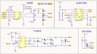
We have tested this circuit and it is working stable. So we need suggestion regarding the CS test. If input resister effected in the CS test then you should suggest me. Other then please provide me the CS test suggestions.
XTR115 4-20mA transmitter can only have one common GND. It may be located at Vloop side (float the input and XTR115) or Ground the input side and float the Vloop power supply. The circuit will not work if both grounds are used.
For CS testings, the Vloop supply is likely grounded via LISN or CDN. You have to show me how the CS is configured, but this is a typical standard configuration
CDN is electronic test equipment used to couple the disturbing signal to several cables connected to the equipment under test.
We have used the CDN for the CS test. Loop+ and loop- cables are passed in the CDN. I think that is standard method follow by all NABL Labs.
I do not have additional information about your circuit, but the Vloop side does show dual TVS protection, and it should be fairly well protected against overvoltage.
Let us get the circuit working first before we are worry about CS testing.
Yes we have added dual TVS protection used for protected against ESD,Surge,EFT. Tihis three EMC test is passed by this design. We have only issue occur in the CS test.
Hi Darshan,
take care, the Iret pin of XTR115/7 is no signal ground! You must allow this pin to freely float. Don't connect it to signal ground:
Also note, that every current flowing into the Iret pin must be sourced by Vreg or Vref!!!! If you have any other supply voltage driving some input circuitry, you will need to add galvanic isolation. See again figure 3 of datasheet.
Kai
Hi Darshan,
This is proper connection for XTR115/XTR116/XTR117 2-wire 4-20mA transmitter. Please note the GND connection and Floating_GND node, which are not the same ground. In addition, the DAC8551's supply voltage in the reference design is powered by XTR116 IC, not MCU.

I am enclosing series application notes and videos in 2-wire and 3-wire 4-20mA transmitters and its application. Per your design approach, 3-wire XTR111 4-20mA transmitter may be used.

https://www.ti.com/lit/ug/tiduao7/tiduao7.pdf?ts=1660822495809
We have tested this circuit and it is working stable.
The V-to-I conversion is very precise. Say 0-5V is the input to 4-20mA current loop conversion, at Vin = 0.000Vdc, the Iout = 4.000mA, when Vin = 5.000V, Iout = 20.000mA. Below is the error specification in XTR115. You need to place 6.5 digits DMM current meter in series with a load in order to monitor current output. During CS test, what is your load?

If you plot out Vin vs. Iout in Excel, you should get the linear relationship as shown in Green boxes. Please specify your circuit's Vin to Iout conversion relationship.

If you have additional questions, please let us know.
Best,
Raymond
Hi Raymond & Kai,
We passed the CS test on the 4-20mA output signal.
I appreciate for your support.
Thanks
Darshan
Hi Darshan,
We passed the CS test on the 4-20mA output signal.
That's good news
Can you share what modifications you have done?
Kai
Hi Darshan,
This is great news! Please share some of the mods you made to pass with CS compliance test.
BTW, TI also makes great TVS as well. The latest designed TVS, part numbers shown below will outperform some of recommended TVS in our old reference design. Enclosed are some of the datasheet, application notes for your references.
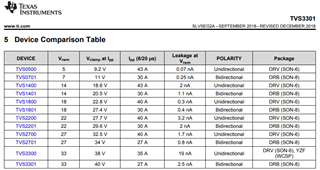
https://www.ti.com/lit/an/slvae53/slvae53.pdf?ts=1661461759768
If you have additional questions, please let us know.
Best,
Raymond
Hi Darshan,
Can you share what modifications you have done?
Thanks for the feedback in passing the CS compliance tests. However, it is equally important to exchange some information how you fixed it and passed the test. This will help us to serve the our fellow engineers better in the future.
Passing CS compliance tests may consist certain "black art". Solutions may be several and we are curious what modifications in the circuit or DUT configuration that made differences.
Best,
Raymond
Hi Darshan,
I am going to close this inquiry. If you have additional questions, please let us know.
Best,
Raymond