Other Parts Discussed in Thread: ADC12DJ3200, LMX2594, ADC12DJ5200RF, LMX2820, LMX1204
Dear TI team,
we are using the LMX2572 PLL to clock some fast TI ADCs.
Two LMX2572 are each located on two different PCBs that are provided with very low skew copies of input signals. These input signals are inherently alligned by a lower-speed PLL on each PCB first, such that SysrefReq always changes on the falling edge of OSCin, so that setup/hold times of the LMX2572 SysRefReq pin are guaranteed to be satisfied under all conditions.
The LMX2572 are in SYSCLOCK repeat mode, with no additional SYSREF delay (JESD_DACy_CTRL at default values from table 140). Both LMX2572 are configured identically, to synthesize one out f three different RefOutA frequencies of either 2.0, 2.5 or 3.2 GHz. RefOutA is then the clock for an ADC12DJ3200, RefOutB is providing the SYSREF signal for the ADC.
Configuration for RefOutA is in such a way, that Synchnonization falls into "Category 2". RefOutA of both LMX2572 is locked and phase stable, no issues here. So synchronization of the two LMX2572 is working.
As far as I understand
1) the SysRefReq pin is first sampled with OSCin. That is, why there are setup/hold timings given in the data sheet.
2) then this sampled version of (1) is somehow further re-clocked with f(INTERPOLATOR)
3) and finally the sampled version of (2) is finally re-clocked to f(RFoutA)
Question 1) Is that assumption correct? Unfortunately there is no internal block diagram showing the exact clocking path.
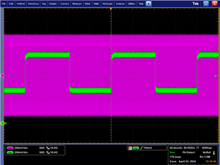
My observation now is that with at least two of the above setups (2.0 GHz and 2.5 GHz RefOutA) the RefOutB outputs of these two LMX2572 are not always aligned, but simetimes are two RefOutA periods apart.
I would expect that on two different LMX 2572 devices (I call them PLL1 and PLL2) , being provided with OSCin and SysRefReq signal that would violate the setup/hold timing of the SysRefReq input pin, that the RefOutB of both devices could be in three different states:
a) PLL1 and PLL2 detect SysRefReg with the same OSCin edge
b) PLL1 detects SysRefReg 1 OCSin clock later than PLL2
c) PLL2 detects SysRefReg 1 OCSin clock later than PLL1
But with our setup of f(SysRefReg) = f(OSCin) / 8 this would result in a much greater difference than just two RefOutA clocks, since the multiplication between OSCin and RefOutA is x80.
But with our setup of not violating the setup/hold times under all conditions, that raises
Question 2) What could the reason be, that whilst input timing is satisfied and RefOutB is not phase stable in relation to SysRefReq ? And could that also happen with our third setup of RefOutA being 3.2 GHz as well and we just have not observed that yet ?
Best regards
Bjoern


