This thread has been locked.

If you have a related question, please click the "Ask a related question" button in the top right corner. The newly created question will be automatically linked to this question.

DAC39J82EVM: Bringing up LMK and DAC SPI

Part Number: DAC39J82EVM
Other Parts Discussed in Thread: DAC39J82,
Hi,
I was trying to bring up SPI interface between DAC39J82(connected to both LMK and DAC) and ZCU106 , meanwhile I was facing few Issues and having few Queries which are mentioned below.
Queries :
  • We considered FMC_SEN_DAC and FMC_SEN_LMK as active low signals which we have connected to a multiplexer and operating either LMK or DAC with the help of a select line .
    •  Query : Can you please tell us the active level of these signals?
  • Taking reference from schematic, we are configured the direction of pins as follows, please confirm whether the directions are fine.
    • FMC_SDIO => Output from FPGA and Input to EVM(connected to CPLD).  
    • FMC_SDO  => Output from EVM and Input to FPGA.
    • FMC_B5   => Output from EVM(DAC) and Input to FPGA.
    • FMC_B6   => Output from EVM(LMK) and Input to FPGA.
    • FMC_SDIO => Output from FPGA and Input to EVM.
    • FMC_SDO  => Output from EVM and Input to FPGA.
    • Query : Please tell which signals we should use for SDIO and SDO for bring up. Also please mention the functionality of all the pins mentioned above.
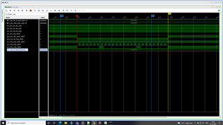
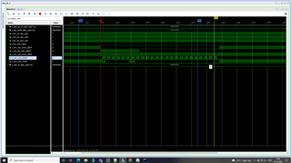
  • We are currently using the SCLK frequency as 6.25 MHz.
    •  Query : Is this okay to use or should we need to reduce even more. As per the data sheet it was mentioned to use maximum of 20 MHz.
  • As per the DAC_39J82 datasheet it was mentioned that SPI interface was three wired by default, and to make it four wired it was suggested to make 7th bit(sif4_ena) of config2 register high.
    • Query : We are currently using 4 wired SPI controller; can you please confirm whether will it work by writing the 7th bit of config2 register high. 
    • Query : Can the 4 wire SPI controller be used from the start ?
Please address the following queries, Looking forward for your reply.
Thanks,
Krishnaveni.
  • Hi Krishnaveni,

    We considered FMC_SEN_DAC and FMC_SEN_LMK as active low signals which we have connected to a multiplexer and operating either LMK or DAC with the help of a select line .
    •  Query : Can you please tell us the active level of these signals?

    The above signals should be active low. 

    6.24MHz should be fine. 

    • Query : We are currently using 4 wired SPI controller; can you please confirm whether will it work by writing the 7th bit of config2 register high. 
    • Query : Can the 4 wire SPI controller be used from the start ?

    The answer to qeustion above is Yes and Yes. 

    Also the post below has the CPLD code and project you can change it as you would like. 

    https://e2e.ti.com/support/data-converters-group/data-converters/f/data-converters-forum/888294/dac37j84evm-configure-cpld-to-receive-spi-signals-from-headers-jp24-and-jp25/3284798?tisearch=e2e-sitesearch&keymatch=DAC38J84%252520CPLD#3284798

    Regards,

    Neeraj 

  • Hi Neeraj,
    • We aren't interested in changing CPLD RTL.
    • We are using 4 wire SPI configuration with FMC_SCK of 6.25 MHz
    • considered FMC_SEN_DAC and FMC_SEN_LMK as active low signals and FMC_DIR_CNTRL pin high while sending data through FMC_SDIO pin.
    • We have performed write operation first by writing 7th bit(sif4_ena) of config2 register.
    • After writing, we read the same register, We observed that FMC_SDO pin was always high, and No toggling was observed.
    • In addition to that we observed FMC_B5 and FMC_B6 were also high, no toggling was observed.
    QUERIES :  
    1. Is the usage of FMC_DIR_CNTRL pin was correct?
    2. How can I confirm whether writing operation was Happened to DAC/LMK Register?
    3. Why FMC_SDO,FMC_B5 And FMC_B6 are always high, wasn't observed any toggling while performing Read operation?
    4. How can we come to know whether CPLD passes the command to LMK/DAC from FMC? 
    5. In CPLD code I havent  seen latching  LMK_SDO  and DAC_SDO by seeing  FMC_SEN_DAC and FMC_SEN_LMK to FMC_SDO  the way happen to FTDI?

    Regards,

     Krishnaveni 

  • Hi Neeraj ,

     In addition to above queries 

    •   We want to access DAC and LMK SPI, dont want to disturb/Change CPLD firmware, how can we access DAC/LMK SPI using FPGA(ZCU106) interfaced over FMC ?

    Regards,

    Krishnaveni

  • Krishnaveni,

    To use the ZCU106 FMC you will have to first verify all of the required signals are routed on the ZCU106 FMC connector. You will need to us the following signals that are shown on sheet 7 of the attached schematic:

    FMC_SDO

    FMC_SEN_DAC

    FMC_SCLK

    FMC_SDIO

    FMC_SEN_LMK

    FMC_DIR_Control

    If the FMC pinouts match between the two boards, you should just have to move the shunt on JP3 to pins 1-2 and provide the required SPI protocol to these signals.

    Regards,

    Jim

    2744.DAC3XJ8XEVM-SCH_D.pdf  

  • Hi Jim ,
    we have Configured FMC SPI Pins Function and IO standard as below
      
    Pin name I/O(for DAC) Description
    FMC_SDO Output  Readback signal from DAC 
    FMC_SEN_DAC Input  Active_low signal DAC chip Select.
    FMC_SCLK Input  Serial clock signal frequency 6.25Mhz    
    FMC_SDIO Input  Serial Address and data for LMK(R/W-1 ,Address - 15 ,Data - 8 ) and
     DAC (R/W-1 ,Address - 6 ,Data - 16 )
    FMC_SEN_LMK Input  Active_low signal LMK chip Select.
    FMC_DIR_CNTRL Input  High when sending Data on FMC_SDIO pin
    FMC_B5 Output  DAC_SDIO read back signal if DAC chip Select FMC_SDIO reflects on DAC_SDIO   
    FMC_B6 Output  LMK_SDIO read back signal if LMK chip Select FMC_SDIO reflects on LMK_SDIO   
      
             Provided each Pin IO standard as above , changed jumper JP3 (1-2 shunt).
             While access the DAC firstly written to config2 SIF4_ena bit , then started reading the Address to get default Value and FMC_SDO pin always low same observed while reading the LMK .
    Query - why FMC_SDO always active low ,while performing Reading operation?
    Query - I have monitored these FMC_B5 and FMC_B6 Pins , why FMC_B5 and FMC_B6 are always active high ?
    I have Attached few screenshots of SPI timing of our setup
                                
                                         Writing to DAC config2  sif4_ena
                          
                                     Reading  DAC config2 register after writing 
    Tested for different Address reading and writing 
    Query - Can you Verify SPI Timing of our setup? 
     
           In our final board we want configure DAC LMK Through SPI from zynq fpga , while configuring LMK and DAC SPI in DAC39J82EVM to Test .
    Facing issues while Reading the Address ,what will be issue ?
    Regards, 
    Krishnaveni
  • Krishnaveni,

    The CPLD source code used by the DAC EVM is attached. This was created by an engineer who no longer works for our group. I do not think the FMC mode was ever tested and may have an issue. You may have to modify the source code and re-program the CPLD to get this to work with your FMC signalstxab_pld.pin. I would suggest monitoring the DAC SPI signals using connector J24 to verify the signals are toggling properly with respect to your signals sent across the FMC before modifying the source code.   

    Regards,

    Jim

    7455.DAC38J84_CPLD.v4174.DAC38J84EVM_CPLD.qar