DS90UB941AS-Q1: DS90UB941 matches DS90UB948 and the 1920x1080 screen is not displayed

Part Number: DS90UB941AS-Q1
Other Parts Discussed in Thread: ALP

Tool/software:

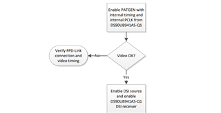
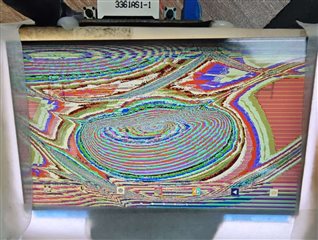
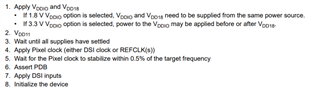
The DS90UB941 configuration register combined with the DS90UB948 outputs 1920*1080 images, 

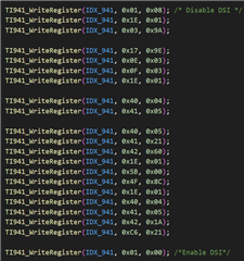
But refer to the programming example of zhcaag5a.pdf manual to modify, the specific register is written as follows, but it can not be displayed on the screen, and read 0x06 register through 941 address can not read the address of the unstring 948, directly read with 948 address, The returned status value is STATUS_I2C_RECEIVED_NACK, there is no idea, please guide to deal with it, thank you

  • Hello!

    I will be referencing the 941AS bring up guide for some further analysis of this setup: DS90UB941AS-Q1 DSI Bringup Guide

    From the script that is provided, I am seeing the following configurations:

    serAddr = 0x18
    
    # Disable the DSI input
    board.WriteI2c(serAddr, 0x01, 0x08) 
    
    board.WriteI2c(serAddr, 0x1E, 0x01) # TX port select, Port 0 selected
    
    # Continuous DSI CLK
    # Dual DSI
    # DSI Port 0
    # Alternate Lines 3D Mode
    # 4 Lanes
    board.WriteI2C(serAddr, 0x4F, 0xDC)
    
    # Dual Config Registers - FPDTX mode = Forced splitter mode
    board.WriteI2C(serAddr, 0x5B, 0x07) 
    
    # Left/Right 3D Processing
    board.WriteI2C(serAddr, 0x56, 0x80) 
    board.WriteI2C(serAddr, 0x32, 0x80) # IMG_LINE_SIZE0 processing
    board.WriteI2C(serAddr, 0x33, 0x07) # IMG_LINE_SIZE1 processing
    # IMG Line processing set to 1920 px
    
    board.WriteI2c(serAddr, 0x1E, 0x01) # TX port select, Port 0 selected (again)
    board.WriteI2C(serAddr, 0x1E, 0x01) # TX port select, Port 0 selected (again)
    board.WriteI2C(serAddr, 0x36, 0x00) # Crop Start X axis (0) - LSB = 0
    board.WriteI2C(serAddr, 0x37, 0x80) # Crop Start X axis (1) - Crop enable, MSB = 0
    board.WriteI2C(serAddr, 0x38, 0x7F) # Crop Stop X axis (0) - LSB = 0111 0111
    board.WriteI2C(serAddr, 0x39, 0x07) # Crop Stop X axis (1) - MSB = 0111
    # Crop start at 0 goes to 1919
    
    board.WriteI2C(serAddr, 0x3A, 0x00) # Crop Start Y axis (0) - LSB = 0
    board.WriteI2C(serAddr, 0x3B, 0x00) # Crop Start Y axis (1) - MSB = 0
    board.WriteI2C(serAddr, 0x3C, 0x37) # Crop Stop Y axis (0) - LSB = 0011 0111
    board.WriteI2C(serAddr, 0x3D, 0x04) # Crop Stop Y axis (1) - MSB = 0100
    # Crop start at 0 goes to 1079
    
    board.WriteI2C(serAddr, 0x40, 0x04) # DSI/DPHY Port 0 Registers
    board.WriteI2C(serAddr, 0x41, 0x05) # DPHY Skip timing
    board.WriteI2C(serAddr, 0x42, 0x1E) # Set to dec = 15
    
    # Enable DSI
    board.WriteI2C(serAddr, 0x01, 0x00) 

    Can you please confirm the DSI configuration being used, the FPD Link topology, and the DSI rate for the appropriate configurations?

    One suggestion I have is to ensure that the correct polarity is selected for the DES / display configuration, this can be done through the following registers on the DSI indirect page registers:

    board.WriteI2C(serAddr,0x40,0x04) # Set HSYNC/VSYNC Polarity DSI0
    board.WriteI2C(serAddr,0x41,0x21) # Set HSYNC/VSYNC Polarity DSI0
    board.WriteI2C(serAddr,0x42,0x60) # Set HSYNC/VSYNC Polarity DSI0

    Additionally, please ensure that the DSI clock settings are configured properly from section 10.2 of the datasheet:

    board.WriteI2C(serAddr,0x40,0x10) # Init DSI Clock Settings (From Section 10.2 of datasheet)
    board.WriteI2C(serAddr,0x41,0x86) # Init DSI Clock Settings (From Section 10.2 of datasheet)
    board.WriteI2C(serAddr,0x42,0x0A) # Init DSI Clock Settings (From Section 10.2 of datasheet)
    board.WriteI2C(serAddr,0x41,0x94) # Init DSI Clock Settings (From Section 10.2 of datasheet)
    board.WriteI2C(serAddr,0x42,0x0A) # Init DSI Clock Settings (From Section 10.2 of datasheet)

    It is also a good idea to digital reset the 948 after initialization in order to restart the AEQ (put this at the end):

    desAddr = 0x58
    
    board.WriteI2C(UB948,0x01,0x01) # Digital reset to restart AEQ 
    

    and read 0x06 register through 941 address can not read the address of the unstring 948, directly read with 948 address, The returned status value is STATUS_I2C_RECEIVED_NACK

    If you cannot read the device ID, it may be that RX Lock is not established. Can you check on the 948 side to ensure the device can be remotely accessed? I am thinking the connection from 941 to 948 may not be established due to hardware configuration. Please check LOCK/PASS status on the 948 to confirm the connection (Pin 1 and Pin 7).

    Let me know if any clarifications are needed here!

    Best,

    Miguel

  • 1.  941 and 948 can be locked after power-on, but TI941_WriteRegister(IDX_941, 0x01, 0x08) when starting to configure the 941 register; And TI941_WriteRegister(IDX_941, 0x4F, 0xDC); So the register will cause the Lock to disconnect, and can not restore the normal connection state, why?
    2.  According to your above Pointers, reconfigure the register 0x41,0x42, then how to configure the corresponding relevant data, because I did not find the reference article, I finally need to output is 1920*1080 screen

  • Hello!

    941 and 948 can be locked after power-on, but TI941_WriteRegister(IDX_941, 0x01, 0x08) when starting to configure the 941 register; And TI941_WriteRegister(IDX_941, 0x4F, 0xDC); So the register will cause the Lock to disconnect, and can not restore the normal connection state, why?

    Yes, this is expected behavior, the first write (0x01=0x08) disables the DSI input, the second write sets the DSI configuration. While the DSI is disabled, there is no input to the RX of the 941 SER, meaning no valid video throughput to the 948.

    At this time, the 948 will sample whether valid video is incoming to certify whether lock is established based on register 0x34 bit 6: RX_LOCK_MODE

    This explains why the lock status is not established as DSI is being configured.

    According to your above Pointers, reconfigure the register 0x41,0x42, then how to configure the corresponding relevant data, because I did not find the reference article, I finally need to output is 1920*1080 screen

    I recommend referring to the DS90UB941AS-Q1 DSI Bringup Guide for specific configuration assistance, as I see splitter mode is being implemented here with cropping to two displays.

    In the debug section, it is recommended to first test the internal pattern generation in order to certify the connection from SER -> DES -> Display is working appropriately, in a topology of SER -> DES -> x1 Display at 1920x1080p, a pattern script can be generated with the register assignments in Exploring the Int Test Pattern Generation Feature of FPD-Link III IVI Devices (Rev. G).

    If you need, I can help generate this script, but I believe the pattern generated will only go to one display (in which I will need the display specification for all timing parameters).

    Please let me know what assistance you may need from here!

    Best,

    Miguel

  • How should I configure which registers? 1920*1080 is the image output, and the clock frequency is 142MHz-158MHz. Can you help me configure the specific registers

  • At present, according to the configuration in the figure, the screen can be displayed, but there is a flower screen, can you help to see is the register configuration cause flower screen? Checked the hardware and found no problems. Thank you

  • Hello!

    I can help you evaluate this configuration; can you please provide an example of flower screen or describe the exact abnormality for documentation purposes?

    Per the debugging flow of the bring up guide (https://www.ti.com/lit/an/snla356/snla356.pdf?ts=1740076915839), I am providing a PATGEN script, which will be internally generated through the 941AS send directly to the 948. Can you please double confirm the topology used by providing a block diagram?

    1920*1080 is the image output, and the clock frequency is 142MHz-158MHz

    I may also need the display timing specifications to prevent any issues from the video timing on the display side, but I have provided a default 1920 x 1080 resolution at 60 fps (148.5 MHz PCLK) PATGEN.

    Please refer to the script below for these register writes:

    devAddr = 0x18
    PGIA = 0x66
    PGID = 0x67
    
    
    board.WriteI2C(0x01, 0x08) # Disable DSI input
    board.WriteI2C(0x1E, 0x01) # TX Port Select = FPD Port 0 Sel
    board.WriteI2C(0x5B, 0x03) # TX Mode = Forced Dual FPD-Link III Transmitter mode
    
    # Populate based on expected display timings
    PGRS =      0x00
    PGGS =      0x00
    PGBS =      0x00
    PGCDC1 =    0x02
    PGCDC2 =    0x98
    PGTFS1 =    0x58
    PGTFS2 =    0x46
    PGTFS3 =    0x80
    PGAFS1 =    0x87
    PGAFS2 =    0x43
    PGAFS3 =    0x2C
    PGHSW =     0x05
    PGVSW =     0x94
    PGHBP =     0x24
    PGVBP =     0x00
    PBSC =      0x1E
    PGFT =      0x0C
    PFTSC =     0x21
    PGTS01 =    0x43
    PGTS02 =    0x65
    PGTS03 =    0x87
    PGTS04 =    0xA9
    PGTS05 =    0xCB
    PGTS06 =    0xED
    PGTS07 =    0x0F
    PGTS08 =    0x00
    PGBE =      0x01
    PGCDC2 =    0x00
    
    board.WriteI2C(devAddr, PGIA, 0x00)
    board.WriteI2C(devAddr, PGID, PGRS) #PGRS
    board.WriteI2C(devAddr, PGIA, 0x01)
    board.WriteI2C(devAddr, PGID, PGGS) #PGGS
    board.WriteI2C(devAddr, PGIA, 0x02)
    board.WriteI2C(devAddr, PGID, PGBS) #PGBS
    board.WriteI2C(devAddr, PGIA, 0x03)
    board.WriteI2C(devAddr, PGID, PGCDC1) #PGCDC1
    board.WriteI2C(devAddr, PGIA, 0x04)
    board.WriteI2C(devAddr, PGID, PGTFS1) #PGTFS1
    board.WriteI2C(devAddr, PGIA, 0x05)
    board.WriteI2C(devAddr, PGID, PGTFS2) #PGTFS2
    board.WriteI2C(devAddr, PGIA, 0x06)
    board.WriteI2C(devAddr, PGID, PGTFS3) #PGTFS3
    board.WriteI2C(devAddr, PGIA, 0x07)
    board.WriteI2C(devAddr, PGID, PGAFS1) #PGAFS1
    board.WriteI2C(devAddr, PGIA, 0x08)
    board.WriteI2C(devAddr, PGID, PGAFS2) #PGAFS2
    board.WriteI2C(devAddr, PGIA, 0x09)
    board.WriteI2C(devAddr, PGID, PGAFS3) #PGAFS3
    board.WriteI2C(devAddr, PGIA, 0x0a)
    board.WriteI2C(devAddr, PGID, PGHSW) #PGHSW
    board.WriteI2C(devAddr, PGIA, 0x0b)
    board.WriteI2C(devAddr, PGID, PGVSW) #PGVSW
    board.WriteI2C(devAddr, PGIA, 0x0c)
    board.WriteI2C(devAddr, PGID, PGHBP) #PGHBP
    board.WriteI2C(devAddr, PGIA, 0x0d) 
    board.WriteI2C(devAddr, PGID, PGVBP) #PGVBP
    board.WriteI2C(devAddr, PGIA, 0x0e)
    board.WriteI2C(devAddr, PGID, PBSC) #PBSC, if not working try both positive AND negative polarity
    board.WriteI2C(devAddr, PGIA, 0x0f)
    board.WriteI2C(devAddr, PGID, PGFT) #PGFT
    board.WriteI2C(devAddr, PGIA, 0x10)
    board.WriteI2C(devAddr, PGID, PGTSC) #PGTSC
    board.WriteI2C(devAddr, PGIA, 0x11)
    board.WriteI2C(devAddr, PGID, PGTS01) #PGTS01
    board.WriteI2C(devAddr, PGIA, 0x12)
    board.WriteI2C(devAddr, PGID, PGTS02) #PGTS02
    board.WriteI2C(devAddr, PGIA, 0x13)
    board.WriteI2C(devAddr, PGID, PGTS03) #PGTS03
    board.WriteI2C(devAddr, PGIA, 0x14)
    board.WriteI2C(devAddr, PGID, PGTS04) #PGTS04
    board.WriteI2C(devAddr, PGIA, 0x15)
    board.WriteI2C(devAddr, PGID, PGTS05) #PGTS05
    board.WriteI2C(devAddr, PGIA, 0x16)
    board.WriteI2C(devAddr, PGID, PGTS06) #PGTS06
    board.WriteI2C(devAddr, PGIA, 0x17)
    board.WriteI2C(devAddr, PGID, PGTS07) #PGTS07
    board.WriteI2C(devAddr, PGIA, 0x18)
    board.WriteI2C(devAddr, PGID, PGTS08) #PGTS08
    board.WriteI2C(devAddr, PGIA, 0x19)
    board.WriteI2C(devAddr, PGID, PGBE) #PGBE
    board.WriteI2C(devAddr, PGIA, 0x1a)
    board.WriteI2C(devAddr, PGID, PGCDC2) #PGCDC2
    
    
    board.WriteI2C(devAddr, 0x65, 0x00)
    board.WriteI2C(devAddr, 0x64, 0x05)


    In this case, you may replace devAddr with IDX_941 as used in your script.

    For further clarification on these configuration registers, please see Exploring the Int Test Pattern Generation Feature of FPD-Link III IVI Devices (Rev. G)

    Since PATGEN will be internally generated at the 941, there is no need for DSI configuration at this time - we are testing the link between SER -> DES -> Display independent of the source.

    Please let me know the results of the testing, then we can proceed to next steps to resolve display abnormalities.

    Thanks,

    Miguel

  • 1、Our project is to input MIPI to LVDS output 1920*1080. Through the example of output internal color bar chart provided by you, the color bar chart can be output normally after testing.1920*1080 is the image output, and the clock frequency is 142MHz-158MHz;
    2、The above is my configuration of the 941 register, through the above configuration, the output screen appears flower screen;

    3、In order to be able to output 1920*1080 video normally, how should I configure, please guide me, more eager,thank you!

  • Hello,

    Thank you for testing this - it appears that the internal PATGEN from the 941AS confirms that the FPD-Link between 941AS and 948 is configured correctly. I will now focus on the DSI RX register configuration.

    Can you please confirm or provide the following information? I will review the code you have provided above in the meantime.

    1. Continuous DSI CLK
    2. Dual DSI (DSI0 and DSI1)
    3. Alternate Lines 3D Mode
    4. Number of DSI lanes per port: 4
    5. DSI rate (Mbps)

    Looking forward to your reply!

    Best,

    Miguel

  • 1、Continuous DSI CLK
    2、Single DSI input, dual output
    3、Not alternate line 3D mode
    4、4 Number of DSI channels
    5、DSI rate (Mbps): 290Mbps

  • Thank you for this information, I will provide feedback for the code above momentarily.

    Best,

    Miguel

  • 5、with fDSI = 492 MHz, 4 DSI data lanes, and DSI reference clock mode, the output video PCLK rate would be 148.5 MHz,

  • I will wait for your feedback, At present, I have no clue to deal with this problem, thank you !

  • Hello,

    Thanks for this information, we will need this for a later step in the debug.

    Through the example of output internal color bar chart provided by you, the color bar chart can be output normally after testing.1920*1080 is the image output, and the clock frequency is 142MHz-158MHz

    For the time being we can now proceed with the flow diagram now that PATGEN from SER is successful (from DS90UB941AS-Q1 DSI Bringup Guide):

    The next script will confirm if the clock is correct and using internal timing (data lanes are not applied).

    devAddr = 0x18
    PGIA = 0x66
    PGID = 0x67
    
    
    board.WriteI2C(0x01, 0x08) # Disable DSI input
    board.WriteI2C(0x1E, 0x01) # TX Port Select = FPD Port 0 Sel
    board.WriteI2C(0x5B, 0x03) # TX Mode = Forced Dual FPD-Link III Transmitter mode
    
    # Populate based on expected display timings
    PGRS =      0x00
    PGGS =      0x00
    PGBS =      0x00
    PGCDC1 =    0x02
    PGCDC2 =    0x98
    PGTFS1 =    0x58
    PGTFS2 =    0x46
    PGTFS3 =    0x80
    PGAFS1 =    0x87
    PGAFS2 =    0x43
    PGAFS3 =    0x2C
    PGHSW =     0x05
    PGVSW =     0x94
    PGHBP =     0x24
    PGVBP =     0x00
    PBSC =      0x1E
    PGFT =      0x0C
    PFTSC =     0x21
    PGTS01 =    0x43
    PGTS02 =    0x65
    PGTS03 =    0x87
    PGTS04 =    0xA9
    PGTS05 =    0xCB
    PGTS06 =    0xED
    PGTS07 =    0x0F
    PGTS08 =    0x00
    PGBE =      0x01
    PGCDC2 =    0x00
    
    board.WriteI2C(devAddr, PGIA, 0x00)
    board.WriteI2C(devAddr, PGID, PGRS) #PGRS
    board.WriteI2C(devAddr, PGIA, 0x01)
    board.WriteI2C(devAddr, PGID, PGGS) #PGGS
    board.WriteI2C(devAddr, PGIA, 0x02)
    board.WriteI2C(devAddr, PGID, PGBS) #PGBS
    board.WriteI2C(devAddr, PGIA, 0x03)
    board.WriteI2C(devAddr, PGID, PGCDC1) #PGCDC1
    board.WriteI2C(devAddr, PGIA, 0x04)
    board.WriteI2C(devAddr, PGID, PGTFS1) #PGTFS1
    board.WriteI2C(devAddr, PGIA, 0x05)
    board.WriteI2C(devAddr, PGID, PGTFS2) #PGTFS2
    board.WriteI2C(devAddr, PGIA, 0x06)
    board.WriteI2C(devAddr, PGID, PGTFS3) #PGTFS3
    board.WriteI2C(devAddr, PGIA, 0x07)
    board.WriteI2C(devAddr, PGID, PGAFS1) #PGAFS1
    board.WriteI2C(devAddr, PGIA, 0x08)
    board.WriteI2C(devAddr, PGID, PGAFS2) #PGAFS2
    board.WriteI2C(devAddr, PGIA, 0x09)
    board.WriteI2C(devAddr, PGID, PGAFS3) #PGAFS3
    board.WriteI2C(devAddr, PGIA, 0x0a)
    board.WriteI2C(devAddr, PGID, PGHSW) #PGHSW
    board.WriteI2C(devAddr, PGIA, 0x0b)
    board.WriteI2C(devAddr, PGID, PGVSW) #PGVSW
    board.WriteI2C(devAddr, PGIA, 0x0c)
    board.WriteI2C(devAddr, PGID, PGHBP) #PGHBP
    board.WriteI2C(devAddr, PGIA, 0x0d) 
    board.WriteI2C(devAddr, PGID, PGVBP) #PGVBP
    board.WriteI2C(devAddr, PGIA, 0x0e)
    board.WriteI2C(devAddr, PGID, PBSC) #PBSC, if not working try both positive AND negative polarity
    board.WriteI2C(devAddr, PGIA, 0x0f)
    board.WriteI2C(devAddr, PGID, PGFT) #PGFT
    board.WriteI2C(devAddr, PGIA, 0x10)
    board.WriteI2C(devAddr, PGID, PGTSC) #PGTSC
    board.WriteI2C(devAddr, PGIA, 0x11)
    board.WriteI2C(devAddr, PGID, PGTS01) #PGTS01
    board.WriteI2C(devAddr, PGIA, 0x12)
    board.WriteI2C(devAddr, PGID, PGTS02) #PGTS02
    board.WriteI2C(devAddr, PGIA, 0x13)
    board.WriteI2C(devAddr, PGID, PGTS03) #PGTS03
    board.WriteI2C(devAddr, PGIA, 0x14)
    board.WriteI2C(devAddr, PGID, PGTS04) #PGTS04
    board.WriteI2C(devAddr, PGIA, 0x15)
    board.WriteI2C(devAddr, PGID, PGTS05) #PGTS05
    board.WriteI2C(devAddr, PGIA, 0x16)
    board.WriteI2C(devAddr, PGID, PGTS06) #PGTS06
    board.WriteI2C(devAddr, PGIA, 0x17)
    board.WriteI2C(devAddr, PGID, PGTS07) #PGTS07
    board.WriteI2C(devAddr, PGIA, 0x18)
    board.WriteI2C(devAddr, PGID, PGTS08) #PGTS08
    board.WriteI2C(devAddr, PGIA, 0x19)
    board.WriteI2C(devAddr, PGID, PGBE) #PGBE
    board.WriteI2C(devAddr, PGIA, 0x1a)
    board.WriteI2C(devAddr, PGID, PGCDC2) #PGCDC2
    
    
    board.WriteI2C(devAddr, 0x65, 0x0C)
    board.WriteI2C(devAddr, 0x64, 0x05)

    While the DSI source is enabled, it will only be providing clock in this scenario, as options of External Clock Source is enabled and Timing is generated and configured internally.

    Please let me know the results of this test, and we may proceed with understanding where the phenomenon is occurring from.

    Best,

    Miguel

  • After writing according to the script you provided, there was no image output on the display screen, and PGTSC did not have the corresponding value in the script you provided. I set PGTSC=0 for the test. The detailed code is as follows:

    TI941_WriteRegister(IDX_941, 0x01, 0x08); /* Disable DSI input */
    TI941_WriteRegister(IDX_941, 0x1E, 0x01); /* TX Port Select = FPD Port 0 Sel */
    TI941_WriteRegister(IDX_941, 0x5B, 0x03); /* TX Mode = Forced Dual FPD-Link III Transmitter mode */

    TI941_WriteRegister(IDX_941, 0x66, 0x00);
    TI941_WriteRegister(IDX_941, 0x67, 0x00);
    TI941_WriteRegister(IDX_941, 0x66, 0x01);
    TI941_WriteRegister(IDX_941, 0x67, 0x00);
    TI941_WriteRegister(IDX_941, 0x66, 0x02);
    TI941_WriteRegister(IDX_941, 0x67, 0x00);
    TI941_WriteRegister(IDX_941, 0x66, 0x03);
    TI941_WriteRegister(IDX_941, 0x67, 0x02);
    TI941_WriteRegister(IDX_941, 0x66, 0x04);
    TI941_WriteRegister(IDX_941, 0x67, 0x58);
    TI941_WriteRegister(IDX_941, 0x66, 0x05);
    TI941_WriteRegister(IDX_941, 0x67, 0x46);
    TI941_WriteRegister(IDX_941, 0x66, 0x06);
    TI941_WriteRegister(IDX_941, 0x67, 0x80);
    TI941_WriteRegister(IDX_941, 0x66, 0x07);
    TI941_WriteRegister(IDX_941, 0x67, 0x87);
    TI941_WriteRegister(IDX_941, 0x66, 0x08);
    TI941_WriteRegister(IDX_941, 0x67, 0x43);
    TI941_WriteRegister(IDX_941, 0x66, 0x09);
    TI941_WriteRegister(IDX_941, 0x67, 0x2C);
    TI941_WriteRegister(IDX_941, 0x66, 0x0a);
    TI941_WriteRegister(IDX_941, 0x67, 0x05);
    TI941_WriteRegister(IDX_941, 0x66, 0x0b);
    TI941_WriteRegister(IDX_941, 0x67, 0x94);
    TI941_WriteRegister(IDX_941, 0x66, 0x0C);
    TI941_WriteRegister(IDX_941, 0x67, 0x24);
    TI941_WriteRegister(IDX_941, 0x66, 0x0D);
    TI941_WriteRegister(IDX_941, 0x67, 0x00);
    TI941_WriteRegister(IDX_941, 0x66, 0x0E);
    TI941_WriteRegister(IDX_941, 0x67, 0x1E);
    TI941_WriteRegister(IDX_941, 0x66, 0x0F);
    TI941_WriteRegister(IDX_941, 0x67, 0x0C);
    TI941_WriteRegister(IDX_941, 0x66, 0x10);
    TI941_WriteRegister(IDX_941, 0x67, 0x00);  // PGTSC
    TI941_WriteRegister(IDX_941, 0x66, 0x11);
    TI941_WriteRegister(IDX_941, 0x67, 0x43);
    TI941_WriteRegister(IDX_941, 0x66, 0x12);
    TI941_WriteRegister(IDX_941, 0x67, 0x65);
    TI941_WriteRegister(IDX_941, 0x66, 0x13);
    TI941_WriteRegister(IDX_941, 0x67, 0x87);
    TI941_WriteRegister(IDX_941, 0x66, 0x14);
    TI941_WriteRegister(IDX_941, 0x67, 0xA9);
    TI941_WriteRegister(IDX_941, 0x66, 0x15);
    TI941_WriteRegister(IDX_941, 0x67, 0xCB);
    TI941_WriteRegister(IDX_941, 0x66, 0x16);
    TI941_WriteRegister(IDX_941, 0x67, 0xED);
    TI941_WriteRegister(IDX_941, 0x66, 0x17);
    TI941_WriteRegister(IDX_941, 0x67, 0x0F);
    TI941_WriteRegister(IDX_941, 0x66, 0x18);
    TI941_WriteRegister(IDX_941, 0x67, 0x00);
    TI941_WriteRegister(IDX_941, 0x66, 0x19);
    TI941_WriteRegister(IDX_941, 0x67, 0x01);
    TI941_WriteRegister(IDX_941, 0x66, 0x1A);
    TI941_WriteRegister(IDX_941, 0x67, 0x00);

    TI941_WriteRegister(IDX_941, 0x65, 0x0C);
    TI941_WriteRegister(IDX_941, 0x64, 0x05);

    TI941_WriteRegister(IDX_941, 0x01, 0x00); /*Enable DSI*/

  • Hi,

    Let us try using this same script by not disabling the clock -> this TX of the DSI is needed to configure the PATGEN:

    TI941_WriteRegister(IDX_941, 0x66, 0x00);
    TI941_WriteRegister(IDX_941, 0x67, 0x00);
    TI941_WriteRegister(IDX_941, 0x66, 0x01);
    TI941_WriteRegister(IDX_941, 0x67, 0x00);
    TI941_WriteRegister(IDX_941, 0x66, 0x02);
    TI941_WriteRegister(IDX_941, 0x67, 0x00);
    TI941_WriteRegister(IDX_941, 0x66, 0x03);
    TI941_WriteRegister(IDX_941, 0x67, 0x02);
    TI941_WriteRegister(IDX_941, 0x66, 0x04);
    TI941_WriteRegister(IDX_941, 0x67, 0x58);
    TI941_WriteRegister(IDX_941, 0x66, 0x05);
    TI941_WriteRegister(IDX_941, 0x67, 0x46);
    TI941_WriteRegister(IDX_941, 0x66, 0x06);
    TI941_WriteRegister(IDX_941, 0x67, 0x80);
    TI941_WriteRegister(IDX_941, 0x66, 0x07);
    TI941_WriteRegister(IDX_941, 0x67, 0x87);
    TI941_WriteRegister(IDX_941, 0x66, 0x08);
    TI941_WriteRegister(IDX_941, 0x67, 0x43);
    TI941_WriteRegister(IDX_941, 0x66, 0x09);
    TI941_WriteRegister(IDX_941, 0x67, 0x2C);
    TI941_WriteRegister(IDX_941, 0x66, 0x0a);
    TI941_WriteRegister(IDX_941, 0x67, 0x05);
    TI941_WriteRegister(IDX_941, 0x66, 0x0b);
    TI941_WriteRegister(IDX_941, 0x67, 0x94);
    TI941_WriteRegister(IDX_941, 0x66, 0x0C);
    TI941_WriteRegister(IDX_941, 0x67, 0x24);
    TI941_WriteRegister(IDX_941, 0x66, 0x0D);
    TI941_WriteRegister(IDX_941, 0x67, 0x00);
    TI941_WriteRegister(IDX_941, 0x66, 0x0E);
    TI941_WriteRegister(IDX_941, 0x67, 0x1E);
    TI941_WriteRegister(IDX_941, 0x66, 0x0F);
    TI941_WriteRegister(IDX_941, 0x67, 0x0C);
    TI941_WriteRegister(IDX_941, 0x66, 0x10);
    TI941_WriteRegister(IDX_941, 0x67, 0x21);  // PGTSC
    TI941_WriteRegister(IDX_941, 0x66, 0x11);
    TI941_WriteRegister(IDX_941, 0x67, 0x43);
    TI941_WriteRegister(IDX_941, 0x66, 0x12);
    TI941_WriteRegister(IDX_941, 0x67, 0x65);
    TI941_WriteRegister(IDX_941, 0x66, 0x13);
    TI941_WriteRegister(IDX_941, 0x67, 0x87);
    TI941_WriteRegister(IDX_941, 0x66, 0x14);
    TI941_WriteRegister(IDX_941, 0x67, 0xA9);
    TI941_WriteRegister(IDX_941, 0x66, 0x15);
    TI941_WriteRegister(IDX_941, 0x67, 0xCB);
    TI941_WriteRegister(IDX_941, 0x66, 0x16);
    TI941_WriteRegister(IDX_941, 0x67, 0xED);
    TI941_WriteRegister(IDX_941, 0x66, 0x17);
    TI941_WriteRegister(IDX_941, 0x67, 0x0F);
    TI941_WriteRegister(IDX_941, 0x66, 0x18);
    TI941_WriteRegister(IDX_941, 0x67, 0x00);
    TI941_WriteRegister(IDX_941, 0x66, 0x19);
    TI941_WriteRegister(IDX_941, 0x67, 0x01);
    TI941_WriteRegister(IDX_941, 0x66, 0x1A);
    TI941_WriteRegister(IDX_941, 0x67, 0x00);
    
    TI941_WriteRegister(IDX_941, 0x65, 0x0C);
    TI941_WriteRegister(IDX_941, 0x64, 0x05);

    The PGTSC was not carried over from the previous write as 0x21 - this is corrected (but has no effect, as auto scrolling is disabled).

    Since the DSI configuration is not disturbed in this setup, please try this sequence:

    This comes from 941 power up sequencing, the suggestion here is to apply the DSI input before initializing with the code above to see if the output will appear. In this way, we can rule out whether the DSI clock is part of the issue in this configuration.

    If that does not work, we will need to evaluate the DSI input further based on this portion of the debug flow diagram (DS90UB941AS-Q1 DSI Bringup Guide):

    In the case the new code and sequencing is unsuccessful, we may try to evaluate the DSI configurations and continuous clock by checking this section:

    I have linked this guide above as well, please let me know if you need any further details testing this.

    If the code and sequence works, we can try the next step which is to use the same code but with external timing input:

    TI941_WriteRegister(IDX_941, 0x66, 0x00);
    TI941_WriteRegister(IDX_941, 0x67, 0x00);
    TI941_WriteRegister(IDX_941, 0x66, 0x01);
    TI941_WriteRegister(IDX_941, 0x67, 0x00);
    TI941_WriteRegister(IDX_941, 0x66, 0x02);
    TI941_WriteRegister(IDX_941, 0x67, 0x00);
    TI941_WriteRegister(IDX_941, 0x66, 0x03);
    TI941_WriteRegister(IDX_941, 0x67, 0x02);
    TI941_WriteRegister(IDX_941, 0x66, 0x04);
    TI941_WriteRegister(IDX_941, 0x67, 0x58);
    TI941_WriteRegister(IDX_941, 0x66, 0x05);
    TI941_WriteRegister(IDX_941, 0x67, 0x46);
    TI941_WriteRegister(IDX_941, 0x66, 0x06);
    TI941_WriteRegister(IDX_941, 0x67, 0x80);
    TI941_WriteRegister(IDX_941, 0x66, 0x07);
    TI941_WriteRegister(IDX_941, 0x67, 0x87);
    TI941_WriteRegister(IDX_941, 0x66, 0x08);
    TI941_WriteRegister(IDX_941, 0x67, 0x43);
    TI941_WriteRegister(IDX_941, 0x66, 0x09);
    TI941_WriteRegister(IDX_941, 0x67, 0x2C);
    TI941_WriteRegister(IDX_941, 0x66, 0x0a);
    TI941_WriteRegister(IDX_941, 0x67, 0x05);
    TI941_WriteRegister(IDX_941, 0x66, 0x0b);
    TI941_WriteRegister(IDX_941, 0x67, 0x94);
    TI941_WriteRegister(IDX_941, 0x66, 0x0C);
    TI941_WriteRegister(IDX_941, 0x67, 0x24);
    TI941_WriteRegister(IDX_941, 0x66, 0x0D);
    TI941_WriteRegister(IDX_941, 0x67, 0x00);
    TI941_WriteRegister(IDX_941, 0x66, 0x0E);
    TI941_WriteRegister(IDX_941, 0x67, 0x1E);
    TI941_WriteRegister(IDX_941, 0x66, 0x0F);
    TI941_WriteRegister(IDX_941, 0x67, 0x0C);
    TI941_WriteRegister(IDX_941, 0x66, 0x10);
    TI941_WriteRegister(IDX_941, 0x67, 0x21);  // PGTSC
    TI941_WriteRegister(IDX_941, 0x66, 0x11);
    TI941_WriteRegister(IDX_941, 0x67, 0x43);
    TI941_WriteRegister(IDX_941, 0x66, 0x12);
    TI941_WriteRegister(IDX_941, 0x67, 0x65);
    TI941_WriteRegister(IDX_941, 0x66, 0x13);
    TI941_WriteRegister(IDX_941, 0x67, 0x87);
    TI941_WriteRegister(IDX_941, 0x66, 0x14);
    TI941_WriteRegister(IDX_941, 0x67, 0xA9);
    TI941_WriteRegister(IDX_941, 0x66, 0x15);
    TI941_WriteRegister(IDX_941, 0x67, 0xCB);
    TI941_WriteRegister(IDX_941, 0x66, 0x16);
    TI941_WriteRegister(IDX_941, 0x67, 0xED);
    TI941_WriteRegister(IDX_941, 0x66, 0x17);
    TI941_WriteRegister(IDX_941, 0x67, 0x0F);
    TI941_WriteRegister(IDX_941, 0x66, 0x18);
    TI941_WriteRegister(IDX_941, 0x67, 0x00);
    TI941_WriteRegister(IDX_941, 0x66, 0x19);
    TI941_WriteRegister(IDX_941, 0x67, 0x01);
    TI941_WriteRegister(IDX_941, 0x66, 0x1A);
    TI941_WriteRegister(IDX_941, 0x67, 0x00);
    
    TI941_WriteRegister(IDX_941, 0x65, 0x08);
    TI941_WriteRegister(IDX_941, 0x64, 0x05);

    This code will then determine if all SoC configurations are coming into the 941 correctly.

    If you have any further questions or concerns, please let me know.

    Best,

    Miguel

  • Using the above code you provided, no image output is displayed

  • For example, I use the address of 948 to read the value of register 0x03, and the return status is STATUS_I2C_RECEIVED_NACK. Is 941 not connected to 948 when configured? This phenomenon will not be the impact of the screen now.

  • Hi,

    When receiving the STATUS_I2C_RECEIVED_NACK, this indicates that there may be an issue with the link between the SER and DES device.

    Is the 948 devices always remotely accessed from the 941 SER? If these transactions are failing, this could indicate an issue on the LOCK stability and status between the SER / DES devices.

    Best,

    Miguel

  • I configured the register of 941 to output the screen of 1920*1080 through the 948 unstring chip. At present, the screen always appears and the register read through the address of the 948 unstring reader always returns STATUS_I2C_RECEIVED_NACK, but the color bar chart can be displayed through the configuration of 941

  • 1、I configured the register of 941 to output the screen of 1920*1080 through the 948 unstring chip. At present, the screen always appears and the register read through the address of the 948 unstring reader always returns STATUS_I2C_RECEIVED_NACK, but the color bar chart can be displayed through the configuration of 941.

    2、948 is set to 0V and R2 is set to 10kΩ. According to the specifications, IDx should be 0x2C. However, I directly connected the MCU to the i2c interface of 948 to read the register of 0xF3 using the address 0x2C, and the return value was STATUS_I2C_RECEIVED_NACK. Using IDx as 0x0C to read the register of 0xF3 does return a successfully readable value, what is the reason? Normal 948 address should be 0x2C, checked the hardware can not find the reason

    3、This is the 941 schematic:

    4、This is the 948 schematic:

  • 5、The color bar map is displayed normally, and the screen output appears on the flower screen. There is a register script in front of it that provides the display effect and the specific configuration of 941

  • Hello,

    Allow me to look into this further, it appears that the mode select strap setting for the 941 does not match the following configuration below?

    4、4 Number of DSI channels
    5、DSI rate (Mbps): 290Mbps

    Mode 0 in this case would be 1 lane, but 4 DSI channels are being used here.

    MCU to the i2c interface of 948 to read the register of 0xF3 using the address 0x2C, and the return value was STATUS_I2C_RECEIVED_NACK. Using IDx as 0x0C to read the register of 0xF3 does return a successfully readable value

    Can you please provide whether the I2C commands from the MCU would read in 7-bit or 8-bit addressing? For example, our ALP tool for the 94x devices will read and communicate in 8-bit IDx addresses:

    ALP Support software | TI.com

    Please let me know, I will continue to evaluate the configuration settings offline, if you are still unable to access the 948 remotely there may be an issue with the backchannel configurations that may need to be evaluated.

    From there, we will continue to look at the DSI CLK source to ensure it is good according to the investigation from reading DSI_VC_DTYPE.

    Best,

    Miguel

  • 1、We have one DSI0 input, two link output, four data channels
    2、Address = 0x4F DSI channel select 1, the screen is not displayed, select 4, the screen is displayed only flower screen
    3、I use an NXP S32K144 chip, which uses a 7-bit address

  • Hi, 

    I see,

    We have one DSI0 input, two link output, four data channels

    Four data channels and dual (two) FPD-Link configuration, you may need MODE_SEL0 = Mode No. 3

    • Pull up resistor would need to be 51.1 kΩ, pull down resistor needs to be 40.2 kΩ
    • Using pull up of 10k with no pull down resistor will enable splitter mode (not suitable for dual link)

    MODE_SEL1 is also set to Mode 7, meaning the DSI will be disabled upon startup.

    • Additionally, a change will be made but the device should use Mode 5 instead for both STP and Coax configurations (this will be updated in future revisions of the data sheet).
    Address = 0x4F DSI channel select 1, the screen is not displayed, select 4, the screen is displayed only flower screen

    I believe this is progress; the lanes should be selected at 4 in order to get any data - but maybe a configuration is causing the flower screen.

    1. Are you able to provide waveforms to certify the incoming clock and data to the RX is meeting 941AS specifications?
    2. Are you able to read indirect page register DSI_VC_DTYPE?
      1. Write 0x40 = 0x04 for DSI Port 0 
      2. Write 0x41 = 0x2A
      3. Read 0x42 (DSI_VC_DTYPE)|
        Example: 
        TI941_WriteRegister(IDX_941, 0x42, 0x04);
        TI941_WriteRegister(IDX_941, 0x41, 0x2A);
        TI941_ReadRegister(IDX_941, 0x42);
    I use an NXP S32K144 chip, which uses a 7-bit address
    Using IDx as 0x0C to read the register of 0xF3 does return a successfully readable value, what is the reason?

    I agree that this is not one of the available addresses on the 948, and is unusual behavior. I am unsure about the reason that only 0x0C works to read the I2C address, are you certain that the address being read here is not the 7-bit address of the 941AS?

    To verify this, you can read register 0x00, it should return the programmed IDx address of that device.

    Best,

    Miguel

  • 1、Are you able to read indirect page register DSI_VC_DTYPE?
        Write 0x40 = 0x04 for DSI Port 0
        Write 0x41 = 0x2A
        Read 0x42 (DSI_VC_DTYPE)
    Reading 0x42 yields a value of 0x3E

  • 1、Are you able to read indirect page register DSI_VC_DTYPE?
        Write 0x40 = 0x04 for DSI Port 0
        Write 0x41 = 0x2A
        Read 0x42 (DSI_VC_DTYPE)
    Reading 0x42 yields a value of 0x3E

  • 2、Are you able to provide waveforms to certify the incoming clock and data to the RX is meeting 941AS specifications?
    This is the waveform of the 941 RX,

    MIPI-CKN to GND test

    3、The comparison diagram displayed on the 1920*1080 display after stringing through 941/948 is as follows. The graph displayed after stringing through is stretched horizontally and vertically with different regular deformations

  • 4、Four data channels and dual (two) FPD-Link configuration, you may need MODE_SEL0 = Mode No. 3

    • Pull up resistor would need to be 51.1 kΩ, pull down resistor needs to be 40.2 kΩ
    • Using pull up of 10k with no pull down resistor will enable splitter mode (not suitable for dual link)

    MODE_SEL1 is also set to Mode 7, meaning the DSI will be disabled upon startup.

    • Additionally, a change will be made but the device should use Mode 5 instead for both STP and Coax configurations (this will be updated in future revisions of the data sheet)

    The hardware is configured according to this information, and the output screen is still a flower screen, which is the same as the previous effect

  • Hi,

    Thank you very much for providing all the additional information about the system.

    The DSI frequency reported in the oscilloscope capture appears to be around 505.35 MHz,

    DSI rate (Mbps): 290Mbps
     fDSI = 492 MHz

    One of these must be incorrect? I believe the data rate to frequency conversion is a multiple of two, so for a data rate of 290 Mbps = approximately 580 MHz DSI clock frequency.

    fPCLK = (fDSI*NLANES)/12

    PCLK = 193.33 MHz

    If this is the case, the UB948 has a PCLK limitation of 192 MHz in dual-link configuration on the FPD-Link RX side, so this may not work.

    - - - - - - - - - - 

    For the DSI frequency that is shown in the oscilloscope capture, this would be a calculation of

    fPCLK = (fDSI*NLANES)/12

    PCLK = 168.45 MHz

    This is fine, but for this configuration T_SKIP is a different number

    With 505.35 MHz / 252.675 Mbps DSI data rate

    TSKIP_CNT = Round(65*fDSI - 5)

    = 28

    board.WriteI2C(serAddr, 0x40, 0x04) # DSI/DPHY Port 0 Registers
    board.WriteI2C(serAddr, 0x41, 0x05) # DPHY Skip timing
    board.WriteI2C(serAddr, 0x42, 0x38) # Set to dec = 28

    With 580 MHz / 290 Mbps DSI data rate

    TSKIP_CNT = Round(65*fDSI - 5)

    = 33

    board.WriteI2C(serAddr, 0x40, 0x04) # DSI/DPHY Port 0 Registers
    board.WriteI2C(serAddr, 0x41, 0x05) # DPHY Skip timing
    board.WriteI2C(serAddr, 0x42, 0x42) # Set to dec = 33

    What is the configuration that allows the screen to produce normal (original drawing)?

    Best,

    Miguel

  • 1、Using 505.35 MHz and 580 MHz calculated values board.WriteI2C(serAddr, 0x42, 0x38) and board.WriteI2C(serAddr, 0x42, 0x42), the effect is still the same, the screen is still displayede

    2、What is the configuration that allows the screen to produce normal (original drawing)?
    The question is to compare the effect of the dot plot I made on the computer and the result displayed on the 1920*1080 screen through the serializer output

    3、This is the register script for the current setup

    status = TI941_WriteRegister(IDX_SER, 0x01, 0x08); /* Disable DSI */
        status = TI941_WriteRegister(IDX_SER, 0x1E, 0x01);
        status = TI941_WriteRegister(IDX_SER, 0x1E, 0x04);
        status = TI941_WriteRegister(IDX_SER, 0x1E, 0x01);
        status = TI941_WriteRegister(IDX_SER, 0x03, 0x9A);

        status = TI941_WriteRegister(IDX_SER, 0x1E, 0x01);
        status = TI941_WriteRegister(IDX_SER, 0x40, 0x05);
        status = TI941_WriteRegister(IDX_SER, 0x41, 0x21);
        status = TI941_WriteRegister(IDX_SER, 0x42, 0x60);

        status = TI941_WriteRegister(IDX_SER, 0x1E, 0x01);
        status = TI941_WriteRegister(IDX_SER, 0x5B, 0x03);
        status = TI941_WriteRegister(IDX_SER, 0x4F, 0x8C);

        status = TI941_WriteRegister(IDX_SER, 0x1E, 0x01);
        status = TI941_WriteRegister(IDX_SER, 0x40, 0x04);
        status = TI941_WriteRegister(IDX_SER, 0x41, 0x05);
        status = TI941_WriteRegister(IDX_SER, 0x42, 0x42);

        status = TI941_WriteRegister(IDX_SER, 0x01, 0x00); /*Enable DSI*/
  • Hi

    Can you please confirm the correct DSI frequency and rate of the SoC and the display timing specifications?

    I am unsure if 505.35 MHz is the correct rate or if 580 MHz is the correct rate.

    I believe we will need to match the SER/DES PCLK rate to the DSI rate, and the PCLK of the SER/DES to the display.

    Thanks,

    Miguel

  • 1、This is DSI frequency and rate of the SoC and the display timing specifications

    disp_timings1: display-timings {

          dsi1_timing0: timing0 {
            clock-frequency = <148500000>;
            hactive = <1920>;
            vactive = <1080>;
            hback-porch = <148>;
            hfront-porch = <88>;
            hsync-len = <44>;
            vback-porch = <4>;
            vfront-porch = <36>;
            vsync-len = <5>;
            pixelclk-active = <0>;
            hsync-active = <0>;
            vsync-active = <0>;
            de-active = <0>;
          };
        };

        //  (1 << 0) - MIPI_DSI_MODE_VIDEO                  /* video mode */
        //  (1 << 1) - MIPI_DSI_MODE_VIDEO_BURST          /* video burst mode */
        //  (1 << 2) - MIPI_DSI_MODE_VIDEO_SYNC_PULSE      /* video pulse mode */
        //  (1 << 3) - MIPI_DSI_MODE_VIDEO_AUTO_VERT      /* enable auto vertical count mode */
        //  (1 << 4) - MIPI_DSI_MODE_VIDEO_HSE              /* enable hsync-end packets in vsync-pulse and v-porch area */
        //  (1 << 5) - MIPI_DSI_MODE_VIDEO_HFP              /* disable hfront-porch area */
        //  (1 << 6) - MIPI_DSI_MODE_VIDEO_HBP              /* disable hback-porch area */
        //  (1 << 7) - MIPI_DSI_MODE_VIDEO_HSA              /* disable hsync-active area */
        //  (1 << 8) - MIPI_DSI_MODE_VSYNC_FLUSH          /* flush display FIFO on vsync pulse */
        //  (1 << 9) - MIPI_DSI_MODE_EOT_PACKET         /* disable EoT packets in HS mode */
        //  (1 << 10) - MIPI_DSI_CLOCK_NON_CONTINUOUS   /* device supports non-continuous clock behavior (DSI spec 5.6.1) */
        //  (1 << 11) - MIPI_DSI_MODE_LPM               /* transmit data in low power */
        dsi,flags = <((1 << 0) | (1 << 1) | (1 << 11) | (1 << 9))>;
        
        // 0 - MIPI_DSI_FMT_RGB888
        // 1 - MIPI_DSI_FMT_RGB666
        // 2 - MIPI_DSI_FMT_RGB666_PACKED
        // 3 - MIPI_DSI_FMT_RGB565
        dsi,format = <0>;

  • Thank you for this information. I will recalculate the intended programmed DSI clk timings and provide you with feedback here.

    In current summary, I am seeing the configuration as successful:

    941AS SER [Internal PATGEN] --> FPD-Link --> 948 --> Display (successfully shows color bars - no flower screen)

    Can you please confirm this so we may focus on SoC DSI TX --> 941AS DSI RX control path?

    Thanks,

    Miguel

  • 1、941AS SER [Internal PATGEN] --> FPD-Link --> 948 --> Display (successfully shows color bars - no flower screen)

    It's like this. It works

  • Hello,

    clock-frequency = <148500000>;
            hactive = <1920>;
            vactive = <1080>;
            hback-porch = <148>;
            hfront-porch = <88>;
            hsync-len = <44>;
            vback-porch = <4>;
            vfront-porch = <36>;
            vsync-len = <5>;
            pixelclk-active = <0>;
            hsync-active = <0>;
            vsync-active = <0>;
            de-active = <0>;
    1、Continuous DSI CLK
    2、Single DSI input, dual output
    3、Not alternate line 3D mode
    4、4 Number of DSI channels
    5、DSI rate (Mbps): 290Mbps

    With the PCLK of 148.5 MHz and 4 data lanes, I believe the DSI frequency should match the following:

    fDSI = (fPCLK * 4) / 12 = 148.5 MHz * 3 = 445.5 MHz

    DSI Datarate = fDSI x 2 = 891 Mbps

    In this case, the TSKIP calculation would be

    TSKIP_CNT = Round(65 * 0.4455 GHz - 5) = 24

    Can you try configuring the SoC to output this 891 Mbps data rate per lane, and also change this Tskip value?

    board.WriteI2C(serAddr, 0x40, 0x04) # DSI/DPHY Port 0 Registers
    board.WriteI2C(serAddr, 0x41, 0x05) # DPHY Skip timing
    board.WriteI2C(serAddr, 0x42, 0x30) # Set to decimal value 24

    Since the clock is continuous, I am assuming that the SoC is outputting in Non-burst mode, please correct me if I am wrong - there is a different configuration needed entirely for Burst mode.

    Best,

    Miguel

  • 1、It should be non-burst mode, due to the urgent development task, the temporary use of this set of hardware only replaces 941 and 948, replaced by other brands of serial chips can normally output 1920*1080 screen, and display normally, using TI 941/948 no matter how to adjust the screen is a display screen, but the color bar can be displayed normally. Contact the local FAE for support, they do not do offline support for us, so can only rely on online technical support

  • Hello,

    Can you please refer me to the local FAE you have contacted? We will discuss with them about getting you dedicated support for this debug. I will continue supporting you here in the meantime.

    Have any of the previous suggestions been implemented on the Source?

    Best,

    Miguel

  • We contacted colt-zhang, and fed back the problem to him at that time, asking him to do technical support. The reply from the FAE of TI said that we needed to read the manual by ourselves, and did not provide any support for our problem. After that, we could only look for support online all the time

  • Thank you for your patience.

    I will put together a presentation recollecting all the previous data and next debug steps. I will relay this information to see if onsite support is possible, but I will also share this support debug flow here, allow me to put this guide together.

    Best,

    Miguel