


Hi,
I'm new to digital isolators but have some experience with opto-isolators. To test its functionality, I hooked up ISO7710FD as in the schematic below:
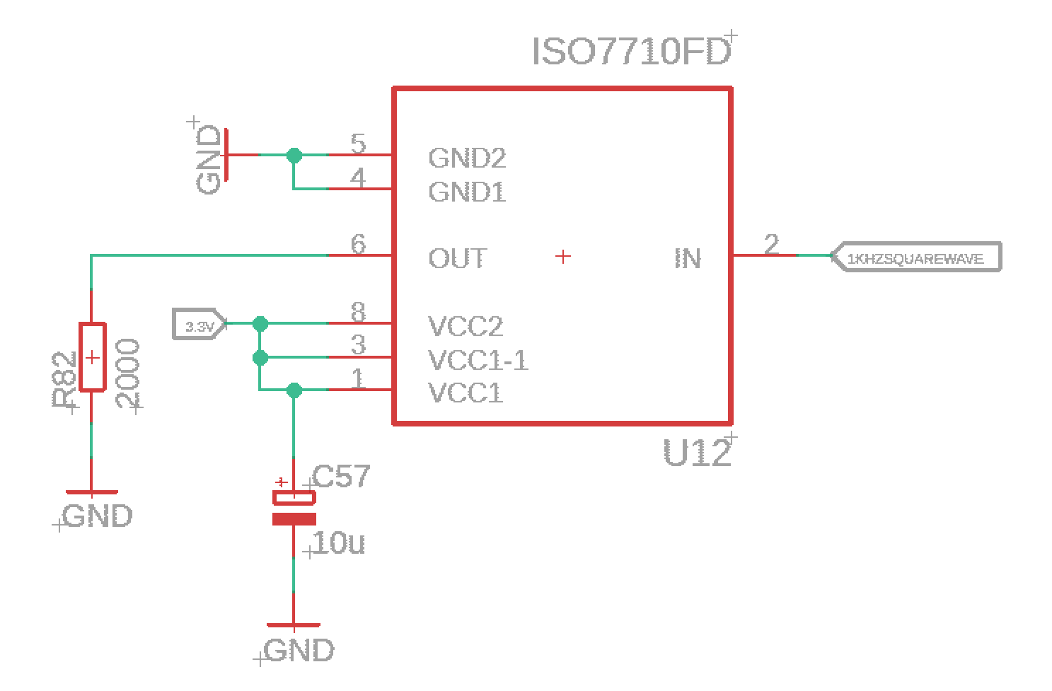
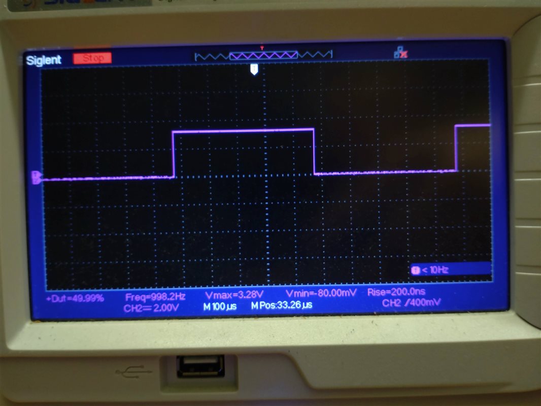
The supplies aren't isolated for testing at the moment. This was my 1KHz 3.3V input squarewave:
I expected the output to be a 1KHz 3.3V squarewave similar to the input, but instead I got a 10KHz 3.3V pulsed output:
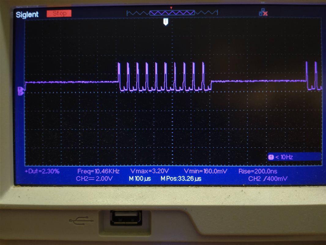
Looking at the datasheet, it seems similar to the carrier signal through the isolation barrier- however from what I understand this should be converted to a squarewave before reaching RXOUT. I've tried different passive components on the output (all with the same 1KHz 3.3V squarewave input):
- 2K Ohm resistor alone resulted in output as shown above
- Adding a 150pF capacitor between output and ground had no effect
- Adding a 0.1uF capacitor between output and ground resulted in a 0.8V ~ 1.8V pulsed output
- No passive components resulted in a constant 3.3V high output signal
Another important factor:
- The device's pins were each reached ~388 Degrees Celsius for 5-10 seconds while soldering to a SOIC-to-DIP adaptor
My diagnosis is that the isolation barrier was damaged during soldering causing the carrier signal to appear at the output, however I'm not entirely sure.
What do you guys think? Has anyone seen such an output while working with digital isolators?
Regards,
MZivcec
