This thread has been locked.

If you have a related question, please click the "Ask a related question" button in the top right corner. The newly created question will be automatically linked to this question.

ISO7763: Entering ESD diodes BV and Max current input Spice .lib file

Part Number: ISO7763
Other Parts Discussed in Thread: PSPICE-FOR-TI, ADC128D818

The ISO7763 has esd protection diodes, but a Vmax and Vmin is specified as well as a current max IN in the input and output pins.  The max output current is 2mA and the max input current is 2µA.

We have a resistive divider network attenuating the input signal (highest I/P) to ±10 V without ISO7763.  Connect the ISO 7763 and the input is limited to 3 or 4 V and input pin current is higher than 2µA.  the corresponding output pin voltage is good.  We are exceeding the Max Vin and input current on the pin, but the part simulates fine.  It would appear that the spice model assumes the device is operating in the proper range.

I need to add the diode BV which is 6V. Vfb appears to be 0.5. I need to include the max diode current 2µA too. The ISO7763 model appears to run on the correct IDEAL conditions. How do I incorporate these parameters into the model to show real word results?  I assume I would add them in the INPUT subcircuit in the ISO7763 .lib file.  

I called the tech support line.   I was told to submit a ticket.  I submitted a ticket, and now I am told to submit another ticket to a different group.  I really need an answer how to do this.  

Sincerely,

Joe

  • Hi Joseph,

    Thanks for reaching out.

    Please note that the spice models are usually developed to simulate the device behavior in the recommended operating conditions only. The device behavior outside the recommended operating conditions is usually not defined and hence, is not modeled into the spice models. Hence, it is possible to see the device continue to operate fine even outside the recommended operating conditions.

    We have a resistive divider network attenuating the input signal (highest I/P) to ±10 V without ISO7763.  Connect the ISO 7763 and the input is limited to 3 or 4 V and input pin current is higher than 2µA.

    Could you please share the schematic showing the resistive divider referenced above to under this statement correctly?


    Regards,
    Koteshwar Rao

  • Yes, I know the spice model does that.  I want to alter the esd diode parameters incorporate the behavior.  How do I do this?

  • Hi Joseph,

    The diode "Dbreak" used in the .lib file is the default diode with default parameters. If you would like to use a custom diode with user defined parameters, then you can define a custom diode .MODEL and use that model name in place of Dbreak in all the sub circuits where you want this diode to be used.

    Let me know if this answers your question, thanks.


    Regards,
    Koteshwar Rao

  • Again, I need to know how to write the statement, and where to add the statement in the ISO7763 Spice .lib model downloaded from TI website.

    The ISO7763 Pspice model has many sub circuits.

  • Hi Joseph,

    Thanks for clarification, I can help you with the actual code to include in the model to allow customization of parameters of the diode. Please find below the code for customizing various parameters of a diode.

    .SUBCKT CDIODE_P np nn PARAMS: 
    + I_Rev_Leak=1e-5 
    + CT_Zero_Volts=300pF 
    + V_BR=600
    + Vj_Knee = 0.90
    + Vj_Spec = 1.6
    + If_Spec = 6
    .PARAM VJ_nom = 0.35
    .PARAM Rs_eq  = {ABS((Vj_spec - Vj_Knee)/If_Spec)}
    .PARAM V_int = {ABS(Vj_Knee - VJ_nom)}
    V_D1 = np np_1 {ABS(V_int)}
    D1 np_1 nn D1exp 
    .model D1exp D Is={I_Rev_Leak} Cjo={CT_Zero_Volts} Rs= {Rs_eq} BV={V_BR}
    .ENDS

    This you can place between subckt OUTPUT and subckt SCHEMATIC3. You can edit V_BR from 600 to 6 like you requested and also modify any other parameters in this subckt.

    Please also make sure to replace all instances of Dbreak with CDIODE_P in subckt INPUT and subckt OUTPUT so that this custom diode is used in place of the standard diode Dbreak.

    Let me know if you have any further questions, thanks.


    Regards,
    Koteshwar Rao

  • Is the diode BV 6 V?  I assumed that because the Vinx is 6V and the esd diode connected to ground in the picture is reversed biased.  Might be a design engineer question.

    When I insert this new code, do I give it a new name or just add the code?

  • Hi Joseph,

    Is the diode BV 6 V? 

    I am assuming you meant to ask for the reverse breakdown voltage of the ESD bypass diodes inside ISO7763. These diodes have a reverse breakdown voltage of slightly higher than 6V but for practical purposes and for simulation, you can assume a value of 6V.

    When I insert this new code, do I give it a new name or just add the code?

    It is upto you to either keep the same name or give a new one. But since this is a custom model file which is not part of PSPICE-FOR-TI default library, you would have to import it like a third party model. In case if you are not familiar with importing third party models, the below training tutorial video should assist you with that.

    https://training.ti.com/pspice-ti-3rd-party-model-import

    As stated in the above training video, while adding the .lib file it is also important to associate it to .old symbol file. The .olb file that you have for ISO7763 can be used as the symbol to associate it to the new model that you are trying to import. This does require you to follow all the steps carefully, failure to do so could lead to errors.

    To further assist you, I have created two custom .lib files with two different implementations for simulating ISO7763 with a custom diode whose reverse breakdown voltage (BV) can be changed as per your need. Please find the files attached below.

    ISO7763_CDIODE_P_1.lib  ISO7763_CDIODE_P_2.lib

    I have also simulated the above and they work fine for recommended operating voltages.

    Let me know if you have any further questions, thanks.


    Regards,
    Koteshwar Rao

  • Thank you.

    I am trying to simulate at what input voltage or input pin current the esd diode will stop limiting the input voltage.  The max pin Voltage is 6V, or vcc+0.5.  I need to determine what that upper limit is. The max pin current is 10µA.  I assume once the esd diode are forward biased then the question shifts to when the pin current exceeds 10µA (on the VIN and 20mA on Vout.

    Is this the correct way to view the issue?

  • Hi Joseph,

    Thanks for additional inputs.

    Is this the correct way to view the issue?

    I am afraid not. I am not quite sure what exactly you are trying to simulate or evaluate. A detailed and clear explanation on your needs / requirements will help resolve the issue sooner.

    The diodes that you see at the input pins are the ESD bypass diodes. i.e., these diodes are meant to bypass any HBM ESD transients at the input / output pins to their respective VCC/GND pins and clamp them to VCC+0.5V for positive ESD transients and to -0.5V for negative ESD transients so that these HBM ESD transients do not damage input/output pins. They are specifically designed to only support protection against HBM and CDM ESD events and do not provide any protection for IEC ESD (which is a much stronger ESD), Surge, overvoltage transient or any continuous overvoltage.

    Overvoltage of any kind (transient or continuous) other than HBM and CDM applied to the pins will lead to current flowing through the diode. Since the diode is not designed for such operation, its reliability will be severely affected and it might not support full device lifetime. Failure of ESD bypass diode could lead to a short between I/O pin and VCC/GND.

    I am trying to simulate at what input voltage or input pin current the esd diode will stop limiting the input voltage.

    Did you mean to ask at what input voltage does ESD bypass diode start bypassing or clamping input to VCC or GND?
    The answer is VCC+0.5V and -0.5V. There is no limiting of input current, any continuous current through ESD bypass diode will affect its reliability.

    The max pin current is 10µA.  I assume once the esd diode are forward biased then the question shifts to when the pin current exceeds 10µA (on the VIN and 20mA on Vout.

    I believe you have incorrect understanding of the input current spec of ±10µA. This is max current consumed by all the input pins under recommended operating conditions. i.e., all the inputs have high input impedance and hence, when a HIGH input signal is applied you will see a max of 10µA into device input pin. Typically, this current will be 1µA or less than that. With sufficient margin, we claim 10µA.

    ±10µA current spec is not the current through ESD bypass diodes. Current through ESD bypass diodes only flows through when recommended operations are exceeded and this happens when HBM and CDM ESD events happen at the input pins. ISO7763 I/Os are designed for 6kV HBM ESD, the current flowing through the ESD bypass diode during this time is going to be between 3A and 5A for a few tens of nanoseconds. Although this seems like a large current, the diode cannot handle any continuous current.

    I would also like to mention that this ESD bypass diode design approach is not unique to ISO7763, such ESD designs are common across most digital device I/Os like MCUs, ADCs, transceivers, logic devices, among others. Even operational amplifiers usually have similar ESD structures.

    Hence, I do not recommend trying to simulate anything around these ESD diodes. Since we do not guarantee device operation for any overvoltage conditions at the I/Os, I will not be able to help you with good answers on simulation questions related to such events.

    I hope this post gives you clarity on operation of device I/O ESD diodes purpose and function and helps you make better decision in simulating device operation under normal test conditions. Thanks.

    You have a great weekend!


    Regards,
    Koteshwar Rao

  • I hope you had a great weekend too.

    Datasheet pg 12 states the min/max input current as ±10µA @ INx.  INx means each pin current not total current of all pins.

    The datasheet clearly states the MAX PIN Voltage- VCCi+0.5V and Min pin voltage= -0.5V.  This clearly states the max esd diode forward bias is 0.5V.  Looking at the esd diode cathode connected to pin on pg2, the max reverse bias applied to the pin is 6V.  So each diode max breakdown voltage is 6V or somewhere close to that when the VCC is ~6V as the absolute max value listed in the datasheet.  When clearly when VCC is < than 6V, then the esd diode with anode connected to pin is ~VCC-6V.

    Fig 23 on pg 25 clearly shows the esd diodes.  The esd diodes will act as limiting diodes until esd diodes reaches its max forward bias current.  Many engineers use this aspect.  These engineers conclude that ±10V can be applied to the input pin and the pin voltage will be limited to VCC +0.5 OR -0.5 on the negative swing, but the esd diode forward bias current is not included in this ASSUMPTION.

    I should be able to include the esd model and clearly show the ISO7763 will not operate VCC + x higher than supply voltage or 0 - y volts below ground.

    So, I can take a ±15V Vpulse apply is to a voltage divider network R1 =50kΩ and R2=100kΩ and R2 connected to +3.3VDC instead of ground and show through simulation the ISO7763 will not operate properly.  We are engineers so we use math (formulas) or simulations (another math form) to prove things not opinions.

    The model provided in last discussions does not work with a resistive divider network applied above even when using Vin-=0V and VCC=3V.  

    This would go so much easier with a call.  

  • look at ADC128D818 datasheet note 5 page 5.

  • Hi Joseph,

    Thanks for further inputs, please see my comments below.

    Datasheet pg 12 states the min/max input current as ±10µA @ INx.  INx means each pin current not total current of all pins.

    Your understanding is correct. These are the maximum input current values into each individual INx pins. But please note that these are only the currents under recommended operating conditions as stated in the headnote of each table.

    The esd diodes will act as limiting diodes until esd diodes reaches its max forward bias current.

    Your understanding is correct, the ESD diodes act as clamping diodes. But please note that these ESD diodes and are designed to clamp ESD pulses at the input pulse.
    What happens if one applies a continuous DC voltage?
    Since these are basically diodes, they will still clamp input voltage. But since they are not rated for such operation, they can get damaged and/or their reliability gets affected.

    These engineers conclude that ±10V can be applied to the input pin and the pin voltage will be limited to VCC +0.5 OR -0.5 on the negative swing

    Yes, the ESD diodes will do the same. But like I mentioned earlier, the diode are not rated for such operations and hence, could get damaged anytime and/or their reliability gets affected.

    the esd diode forward bias current is not included in this ASSUMPTION

    They are rated to support 3A to 5A of current for a few tens of nanoseconds. If you ask what continuous current the diodes can reliably handle for their life, I would say 0mA because they are not designed for continuous current operation.
    Does this mean if you pass a few mA of current, do they get damaged immediately?
    Not necessarily, they can get damaged over a period of time but the lifetime of device will be severely affected by doing so.

    I should be able to include the esd model and clearly show the ISO7763 will not operate VCC + x higher than supply voltage or 0 - y volts below ground.

    The ESD diodes will not let the input voltage exceed VCC+0.5V and -0.5V till they get damaged. I believe you have already seen this behavior in your earlier simulations with existing ISO7763 model.

    So, I can take a ±15V Vpulse apply is to a voltage divider network R1 =50kΩ and R2=100kΩ and R2 connected to +3.3VDC instead of ground and show through simulation the ISO7763 will not operate properly.  We are engineers so we use math (formulas) or simulations (another math form) to prove things not opinions.

    I am sorry, from the above description I couldn't make out what connection are made to VCC or INx of ISO7763.

    The model provided in last discussions does not work with a resistive divider network applied above even when using Vin-=0V and VCC=3V.

    Could you please share a screenshot of the schematic or waveform so that I understand the connections?

    look at ADC128D818 datasheet note 5 page 5.

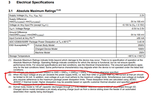
    Thanks for pointing this out. The datasheet of ADC128D818 does ask one to externally limit the current to 5mA to avoid damage. Please also note that they also mention in footnote (3) that operating device in such use conditions for extended periods might affect reliability, also shown below for your reference.

    1. Exposure to absolute-maximum-rated conditions for extended periods may affect device reliability.

    This applies to ISO7763 as well but we do not like to claim 5mA as safe current through the diode as we cannot define what is considered extended period. Hence, we discourage operating in such conditions.

    Let me know if you have further questions, thanks.


    Regards,
    Koteshwar Rao
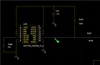
  • ±X is applied to right of 49kΩ resistor.

    ESD diodes work by how much energy can be applied: V*I*time.  What i am referring is a continuous signal 50% duty cycle that can vary from ±3V to ±15V (RS232 standard).  Many engineers think, oh esd diodes will limit to 3.3VDC, in the attached picture.  But, that is not the total story.  I have to include the Max current into the pin.  In the ISO7763 figure 23 pg 25, a series resistor and pull up resistor (or pull down) is after the first set of esd diodes.  

    The max pin current is ±10µA.  Based on the fig 23, not all the pin current is the esd diode forward bias.  So, I should be able to increase the Vin from ±3V to ±15 in say 1V steps and monitor when pin current is 10µA,  The assumption is that when the esd diodes are turned on that the majority of the pin current will flow through them because they have lower resistance on than the resistors.

    This might not be a valid assumption.  It might be that the 10µA is only normal operation.  Then maybe through simulation I can prove when the ISO7763 fails.  The ADCXXXX lists that at 5mA.  The ISO7763 does not.  I realize that the chip will probably be damaged.  That is what I am trying to show others.

    I cannot make the circuit simulate with the esd diode changes when connected like the attached picture.

  • This is from ADC128Dxxxx datasheet confirming my analysis.  It will be different from part to part depending on esd diode size, This part actually lists the max input current.

  • Hi Joseph,

    Thanks for sharing the schematic.

    What i am referring is a continuous signal 50% duty cycle that can vary from ±3V to ±15V (RS232 standard)

    Like I mentioned earlier, we do not guarantee device function outside of recommended operating conditions. The simulation models are also designed to operate under recommended conditions only. Hence, I cannot comment for the operations outside of these conditions.

    So, I should be able to increase the Vin from ±3V to ±15 in say 1V steps

    Since this is outside device spec, I wouldn't be able to comment on device functionality under these test conditions.

    The ADCXXXX lists that at 5mA.  The ISO7763 does not.

    Like I already clarified in my previous post (see below), ADC128D818 states customers to limit current through diode to 5mA while we ask customer to limit it to 0mA for the reasons stated below.

    look at ADC128D818 datasheet note 5 page 5.

    Thanks for pointing this out. The datasheet of ADC128D818 does ask one to externally limit the current to 5mA to avoid damage. Please also note that they also mention in footnote (3) that operating device in such use conditions for extended periods might affect reliability, also shown below for your reference.

    1. Exposure to absolute-maximum-rated conditions for extended periods may affect device reliability.

    This applies to ISO7763 as well but we do not like to claim 5mA as safe current through the diode as we cannot define what is considered extended period. Hence, we discourage operating in such conditions.

    I cannot make the circuit simulate with the esd diode changes when connected like the attached picture.

    I have simulated the circuit under recommended operating conditions and it has worked fine. The tool probably doesn't allow you to simulate outside these specs, maybe that's why you are not able to simulate. 

    Let me know if you have any further questions, thanks.


    Regards,
    Koteshwar Rao

  • We are back where we first started.  I already know this part is not operating properly.  Engrs think esd diodes are the same as limiting diodes; they are not.  I have to prove this with mathematical analysis or simulations.

    I need this info from TI: 

    1.  ESD diodes full Pspice model

    2.  The max pin current when the esd diode is forward biased.

    The ADC128D818 clearly gives this information: Section 7.1 pg 5 note 5 & Section 7.5 pg 6 note 1.

    The ISO7763 does not give any information like the ADCXXX.  This is the info I need to show in a sim to others that we cant do this.  

  • Please read the app note starting below Fig 2:  It is design engr responsibility to know max current the pin can have.  I showed you TI datasheet that lists that.  This appears not to be a standard note for all datasheets.  I need the esd diode details so I can determine this.  

    https://en-support.renesas.com/knowledgeBase/19917727

  • Hi Joseph,

    Thanks for further inputs.

    I believe I tried to provide all the information that has been requested wherever it is available. Please allow me address the requests that you have made in the last two posts.

    I have to prove this with mathematical analysis or simulations.

    As mentioned earlier, I would like to reitirate that the PSpice model doesn't behave like the actual device outside its recommended operating conditions. Hence, you will not be able to prove device failure through simulations. You would have to consider laboratory testing for this.

    1.  ESD diodes full Pspice model

    I am afraid I will only be able to provide PSpice model for the orderable device, ISO7763 which simulates device behavior accurately within recommended operating conditions, as stated earlier.

    2.  The max pin current when the esd diode is forward biased.

    I believe you are seeking for a max continuous forward current specification for the ESD diode. I would like to reiterate again that the ESD diode isn't designed or characterized for continuous current and hence, I do not have a value to share with you. Like I have already mentioned earlier, as a general rule-of-thumb, you can use the same current as ADC128D818 but do note that this is not a specification. The link that you provided to a knowledge base article also clearly states that this is not a specification but a general rule of thumb.

    The ADC128D818 clearly gives this information: Section 7.1 pg 5 note 5 & Section 7.5 pg 6 note 1.

    Like I have already pointed out, the datasheet of ADC128D818 mentions 5mA as a guideline but not quote it as a continuous current rating. Please see footnote (3) in section 7.1 (also copied below for your reference).

    I hope I have answered your questions to your satisfaction, thanks.


    Regards,
    Koteshwar Rao