1) Regarding the TMS320F28384S, what are the precautions when using CM (Connectivity Manager)? Is it necessary to create a project that is different from the DSP side (C28 CPU)?

2) I would like to know the points to note when creating a memory map and appropriate allocation when the CM (connectivity manager) and DSP side (C28 CPU) coexist. I would like to know RAM and flash separately.

3) Is it possible to run the program only on the DSP side (C28 CPU)? Conversely, what should I do on CCS when debugging both CM and CPU?

4) I would like to know how CM and CPU memory are shared. Is it possible to share a global variable and make it behave like accessing it at the same time? "In that case, what would be a specific description example?"
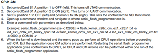
5) I saw a description that CM always needs reset release from CPU. Does this mean that there is no choice but to start booting from the real CPU? Also, if you want to consider the FW update mechanism, is it impossible to implement a method such as stopping the CPU from the CM and updating the CPU side?