Other Parts Discussed in Thread: C2000WARE, UNIFLASH
Tool/software:
Hi TI team,
I'm studying the TMDSCNCD28P65X control card and trying to program some example code from C2000Ware_5_04_00_00 using CCS version is 12.8.1.00005
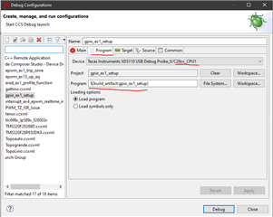
I've imported the example project: gpio_ex1_setup. And it build successfully.
But I can't load it successfully. The CCS log are shown below:

""""""""
C28xx_CPU1: GEL Output:
Memory Map Initialization Complete
C28xx_CPU1: GEL Output: ... DCSM Initialization Start ...
C28xx_CPU1: GEL Output: ... DCSM Initialization Done ...
C28xx_CPU1: GEL Output:
CPU2 is out of reset and configured to wait boot.
(If you connected previously, may have to resume CPU2 to reach wait boot loop.)
C28xx_CPU1: If erase/program (E/P) operation is being done on one core, the other core should not execute from shared-RAM (SR) as they are used for the E/P code. User code execution from SR could commence after the selected flash banks are programmed.
C28xx_CPU1: Only CPU1 on-chip Flash Plugin can configure clock for CPU1, and CPU2 Flash operations. Plugin automatically configures PLL when CPU1 Flash operations are invoked. However, if users want to do only CPU2 Flash operations without doing a prior CPU1 operation in the current session, they should click on 'Configure Clock' button in CPU1's on-chip Flash Plugin before invoking CPU2 Flash operations. When this button is used, Flash Plugin will configure the clock for CPU1/CPU2 at 200MHz using INTOSC as the clock source. Plugin will leave PLL config like this and user application should configure the PLL as required by application.
C28xx_CPU1: Before doing any flash operations using the flash plugin, (a) Please select which flash banks should be mapped to which CPU (CPU1 vs CPU2) - This selection should be done in CPU1 flash plugin GUI. (b) Please select the flash banks that the user would like the flash plugin to erase (in the CPU1 flash plugin GUI and the CPU2 flash plugin GUI)
C28xx_CPU1: GEL Output: ... DCSM Initialization Start ...
C28xx_CPU1: GEL Output: ... DCSM Initialization Done ...
C28xx_CPU1: GEL Output:
CPU2 is out of reset and configured to wait boot.
(If you connected previously, may have to resume CPU2 to reach wait boot loop.)
C28xx_CPU2: GEL Output:
RAM initialization done
C28xx_CPU2: GEL Output:
Memory Map Initialization Complete
C28xx_CPU2: If erase/program (E/P) operation is being done on one core, the other core should not execute from shared-RAM (SR) as they are used for the E/P code. User code execution from SR could commence after the selected flash banks are programmed.
C28xx_CPU2: Only CPU1 on-chip Flash Plugin can configure clock for CPU1, and CPU2 Flash operations. Plugin automatically configures PLL when CPU1 Flash operations are invoked. However, if users want to do only CPU2 Flash operations without doing a prior CPU1 operation in the current session, they should click on 'Configure Clock' button in CPU1's on-chip Flash Plugin before invoking CPU2 Flash operations. When this button is used, Flash Plugin will configure the clock for CPU1/CPU2 at 200MHz using INTOSC as the clock source. Plugin will leave PLL config like this and user application should configure the PLL as required by application.
C28xx_CPU2: Before doing any flash operations using the flash plugin, (a) Please select which flash banks should be mapped to which CPU (CPU1 vs CPU2) - This selection should be done in CPU1 flash plugin GUI. (b) Please select the flash banks that the user would like the flash plugin to erase (in the CPU1 flash plugin GUI and the CPU2 flash plugin GUI)
C28xx_CPU2: File Loader: Verification failed: Values at address 0x00A800@Program do not match Please verify target memory and memory map.
C28xx_CPU2: GEL: File: D:\Project\Tesseract\TI P65 test\gpio_ex1_setup\CPU1_RAM\gpio_ex1_setup.out: a data verification error occurred, file load failed.
""""""""
However, I can load & verify FW by using UniFlash. (Version 8.8.1.4983)

Can someone please help to check and how to solve it?
Why the CCS cannot debug & load FW?
Thanks.