This thread has been locked.

If you have a related question, please click the "Ask a related question" button in the top right corner. The newly created question will be automatically linked to this question.

MSP430 I2C glitch pulses causing trouble for I2C peripheral chip

Other Parts Discussed in Thread: MSP430F5438A, MSP430F5342

Hello,

This is maybe a question for a TI engineer, or anybody else with a detailed knowledge of the MSP430F5438A's I2C port.

We're using the MSP430F5438A connected to a ZSC31014 bridge amplifier chip using the I2C bus in master mode, from the MSP's port UCB3. Our I2C bus uses 4k7 pullups.

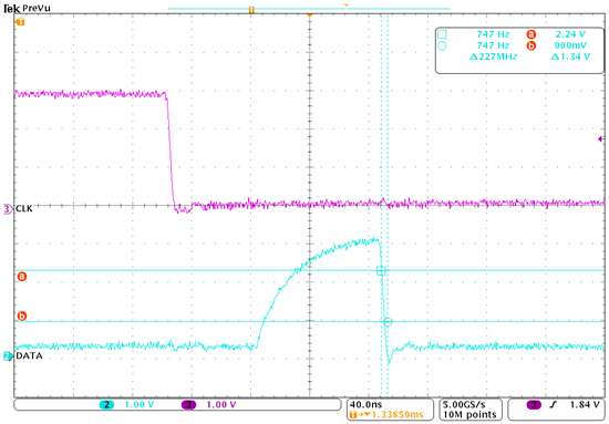
We've been having a problem that the MSP4305438A's I2C port produces a glitch spike on the SDA line, between what we perceive to be the end of each start bit and the beginning of the MSbit 6 of the address byte, as follows:

Zooming in on the glitch pulse:

We fully understand that this glitch spike should not matter to I2C operation. However, unfortunately the ZSC31014 datasheet (on page 24) states that its I2C port departs from the normal I2C specification: "A falling SDA edge is not allowed between the start condition and the first rising SCL edge. If using an I2C address with the first bit 0, SDA must be held low from the start condition through the first bit."

This combination of the MSP430 I2C glitch pulses, and the ZSC31014's susceptibility to them, resulted in us having reliability problems with this chip. Our workaround is to configure the ZSC chip to have an address with its bit 6 set (e.g. we’re now using 0x42) - this turns the glitch pulse into a nice clean "high" bit for the address bit 6 duration, which gets rid of the problematic falling edge.

However, we would like to know if there is any way of stopping the MSP430F5348A's I2C port from generating this glitch pulse in the first place, for I2C addresses below 0x40? For example, any "trick" settings of the MSP430's I2C register settings? Or, are these glitch pulses an unavoidable by-product of the normal MSP430 I2C port operation?

Many thanks in advance,
Bart

(P.S. I've already seen the separate "msp430 I2C glitch / spike issue" forum entry at http://e2e.ti.com/support/microcontrollers/msp430/f/166/t/237128.aspx)

  • BartW said:
    ZSC31014 bridge amplifier chip using the I2C bus in master mode

    First I’m not sure how is the master here, and also generating the clock (and spikes)?

    To suppress the spikes you can add to each device, in both lines a series resistor. In your case with a pull-up of 4K7 and assuming you are using 3.3V a series resistor of about 300 Ohm will be suitable.

  • Hi Leo,

    Thanks for your quick reply. To clarify, the MSP430 is our I2C bus master.

    Thanks also for your suggestion of using 300 ohms series resistors. However, this isn't practical for us because our hardware is already implemented. Our fix of changing the ZSC31014 address to 0x41 does work well, but it has some (fiddly but not critical) roll-out issues for us to change the ZSC chip's I2C address on all of our boards. Therefore, we are hoping that there might be a firmware-side fix (e.g. MSP430 I2C "trick" register settings) to get rid of the glitch. But we are guessing this this glitch is is probably a by-product of the MSP430 I2C peripheral's internal hardware state machine behaviour, and therefore it might not be possible to get rid of it by making firmware changes. Hopefully a TI engineer would be able to clarify this further?

    Best wishes,

    Bart

  • The undershoots are not produced by the device but by the hardware behind. Strange is in your magnified screen-shot there are no undershoots, probe capacitance? But this is not your actual point.

    The short transition on the SDA line might not be nice but they are part of the START arbitration and also fully into the specs of I2C. I don’t think TI can give you a solution, the problem is the ZSC31014 device. Maybe you can solve it by adding a little capacitance on the SDA line (not nice but..).

  • The I2C Data is designed to be driven low (with an open collector) by one of many devices. When none of them is driving it low, it is pulled up (slowly) by a resistor. I think this is what causes the glitch.

    (1) If the address is an odd number such as 0x41, I2C Data is high to begin with. There is no glitch and no changes are needed. Only when the address is even, where I2C Data begins as low, there will be a glitch. I think there is a firmware workaround to avoid that. This workaround is described below.

    (2) The I2C Data and a GPIO share the same pin. We could set up that GPIO as out-low. Normally that shared pin is selected as I2C Data, thus GPIO being out-low is inconsequential.

    (3) However, shortly before point A, as shown in the picture below, the firmware could select that pin as GPIO. And shortly after point B, the firmware could select that pin as I2C Data again. Thus between A and B, that pin is constantly driven low by that GPIO (shown in blue) and no glitch will show.

  • Mm… I don’t know how MSP is exactly handling the signals, but pulling SDA low normally results in a Bus-busy state, A can give a problem. And also B can lead to an arbitrage lost, while SDA remains low and the master is recognizing this as a Start from another master and will give-up.

  • OCY: right. When clock goes low, the data pin is released by the state machine, before it is switched to the state of the bit to output. During this time, the pull-up pulls it up. This is totally valid. During SCL=0, the SDA signal can change as often as it wants.

    However, if the slave is apparently not 100% compliant to the I2C standard, knowing the reasons doesn’t help.

    LEO: the bus is always busy after a start and before a stop is received. It has nothing to do with data held low.

    However, if data is held low while the USCI wants to output a high, this is considered an arbitration loss. Now in this condition, the USCI wants the output to be low. It’s just during the state transition, that the output pin is temporarily released.

    BTW: I see the bit time and the glitch time and the size of the glitch. I’d say, the pull-up is way stronger than required. A larger pull-up might solve the problem, as during the glitch time, voltage won’t rise that fast anymore.

  • Jens-Michael Gross said:
    LEO: the bus is always busy after a start and before a stop is received. It has nothing to do with data held low.

    Pulling SDA low (the time before ‘A’) IS a START condition result Bus-busy!

  • Many thanks for all of your replies. We have decided to use our solution of changing the strain chip address to 0x42 (as I mentioned in an earlier post), which has proved to be a very reliable work-around, after lots of testing.

    A few quick responses to your suggestions:

    • Leo (putting capacitance on the SDA line): Our hardware engineers did actually initially put a 100pf capacitor on the SDA line (the PCB allowed this to be hand-soldered on). This seemed to work for some boards, but was an undesirable solution because we could not be sure of reliability, temperature-dependent behaviour etc
    • old_cow_yellow and others (holding SDA low by changing to GPIO): We did lots of experimentation in this direction in the past, with mixed results. However, the bottom line (I think) is that it would be too fiddly to do this, in terms of getting the timings correct, the potentially different I2C clock rates, possible interrupts disrupting this operation etc. The timings for the firmware control of the SDA pin as GPIO would have to be just right, to correspond to what the I2C peripheral was doing at the same time
    • Jens-Michael: The pulse height was indeed affected by the pull-up resistor value. We use 4k7 pull-ups, which is pretty standard for I2C. However, changing these resistors as a fix could again be unreliable and temperature-dependent etc (the problem was already very intermittent to begin with, for these reasons :))

    Many thanks again to all.

    Best wishes,

    Bart

  • Leo, pulling SDA low by port IO while it has been already pulled low by USCI for start condition, to gap the glitch, leads to bus busy while bus is already busy. That was the idea and suggestion. Of course, simply pulling the line low at some random time is not working and wasn’t suggested.

     BartW, the glitch time is pretty short compared to the I2C clock frequency. So you apparently have a really low capacitance bus. Yes, 4k7 are pretty much standard, but in in most cases, 10k do fine. You can try a combination of both, raising the pull-up and adding some load capacitance to the bus.

    Here’s a nice link:
    Design calculations for robust I2C communications | EDN

  • Bart --

    Thanks for posting this. I ran into the exact same issue with a MSP430F5342 and ZMD ZSC31014 bridge IC. It was not fun to find, the spike amplitude was right where only some PCB assemblies had the issue. It was also narrow enough to be hard to see on the scope.

    In my case, I solved it by bit-banging the I2C to the ZMD to eliminate the spike. Like you, I had a population of devices that were already programmed with a ZMD address that started with '0'.

    Tim

**Attention** This is a public forum