How to use a high side switch (HSS) to implement one fail all fail in a multi-module automotive LED rear light system?
A typical LED based rear lamp, shown in Figure 1, consists of several lamp functions such as tail, stop and turn signals. Based on the shape and design of the lamp, each lamp function could be implemented using multiple LED drivers and LED printed circuit boards (PCBs). Furthermore, each lamp in the rear light is turned on and off by the body control module (BCM).
Figure 1: Rear-lamp and its connection to BCM
A key design requirement in such automotive rear lighting systems is diagnostic solutions to detect LED open, short or single LED short failures. These failure events need to be detected by the BCM so that the driver can be notified of the malfunction via the check engine light.
The BCM detects a failure in the rear light module by measuring the current draw in the control line. In order for the BCM to detect the failure without using high accuracy current sense solution, LED drivers implement a feature called one fail – all fail. With this feature, the LED driver turns off all the LEDs in the specific lamp function, even if one LED fails. That is, if one LED fails, turn off all LEDs.
Many LED drivers have a dedicated “fault” pin which can be interconnected to implement one fail – all fail. However, when the distance between two LED driver PCBs is large within one lamp or even between two lamps, such as a lamp in the fender and a lamp in the trunk, electromagnetic immunity is of concern. A HSS can be effectively used in the solution with its protection features like short to GND and short to battery.
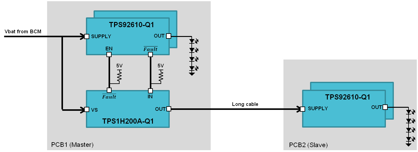
Figure 2 shows a simplified block diagram of HSS in rear light solutions. In this figure, the TPS92610-Q1 is linear LED driver and TPS1H200A-Q1 is HSS device.
Figure 2: Block diagram showing the use of high side switch in rear lamps
The solution works as follows:
The fault pin of the HSS on PCB1 is connected to the enable pin, EN, of the LED driver and the fault pin of the LED driver is connected to output enable pin, IN, of the high side switch. Both signals are pulled up to 5 V to achieve a defined startup. In normal operation, the HSS in PCB1 enables power to the LED driver in PCB2. There are two failures that can occur:
- LED failure in PCB1. When a PCB1 LED failure occurs, the LED channels on PCB1 will be disabled and the LED driver Fault pin goes low. This turns off the HSS, which results in the turning off LEDs in PCB2. That is, failures in PCB1 will also turn off all LEDs in the lamp.
- LED failure in PCB2: When a PCB2 LED failure occurs, the LED driver will turn off the LEDs in PCB2. The current consumption of PCB2 reduces and the HSS in PCB1 detects this as an open load. The HSS fault pin goes low and disables the LED drivers on PCB1. This then turns off the LEDs in PCB1. Thus, failures in PCB2 will turn of all LEDs in the lamp.
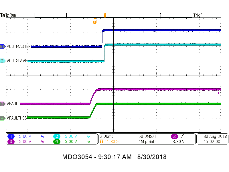
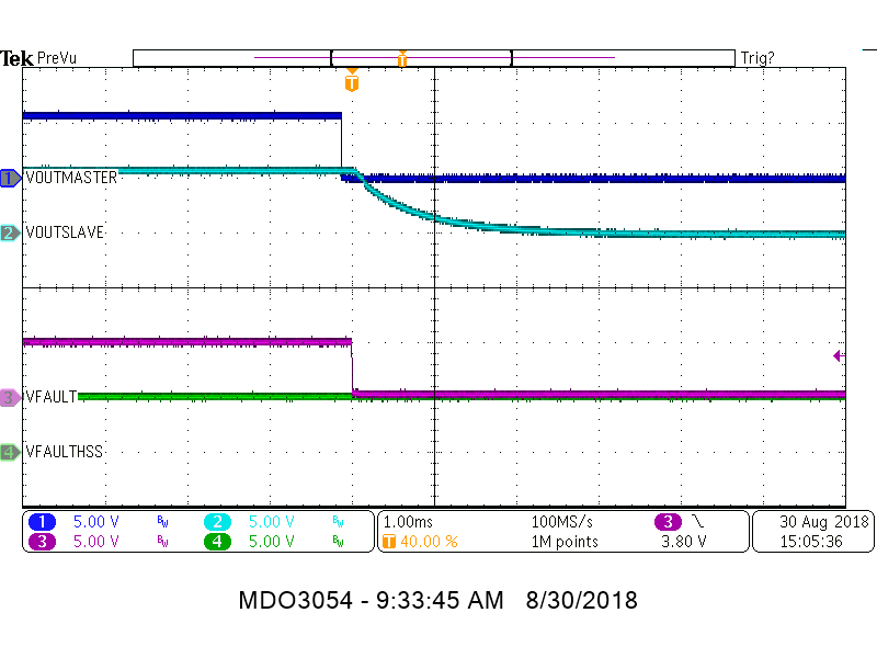
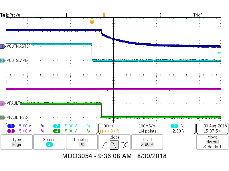
Figures 3, 4 and 5 show the performance of the implementation.
Figure 3 shows the system startup. When power is applied to PCB1, the fault pins of LED driver (CH3) and HSS (CH4) go high and the outputs of the LED drivers (CH1), (CH2) also go high.
Figure 3: System startup (CH1: Vout LED driver PCB1, CH2: Vout LED driver PCB2, CH3: Fault LED driver PCB1, CH4: Fault HSS)
Figure 4 shows the event of short circuit on LED driver output (CH1) on PCB1. In this case the fault signal of LED driver (CH3) on PCB1 goes low and disables the output of the HSS. Thus the output of the LED driver (CH2) on PCB2 goes low.
Figure 4: LED short on PCB1 (Master) (CH1: Vout LED driver PCB1 (Master), CH2: Vout LED driver PCB2 (Slave), CH3: Fault LED driver PCB1, CH4: Fault HSS)
Figure 5 shows a short circuit event on the LED driver output (CH2) on PCB2. In this case the HSS in PCB1 detects this as an open load. The HSS fault pin (CH4) goes low and disables the LED drivers on PCB1. Thus the output of the LED driver (CH1) on PCB1 goes low.
Figure 5: LED short on PCB2 (Slave) (CH1: Vout LED driver PCB1, CH2: Vout LED driver PCB2, CH3: Fault LED driver PCB1, CH4: Fault HSS)
References:
- Review the rear light system block diagram
- Learn more about TPS1H200A-Q1 high side switches
- Learn more about TPS92610-Q1 LED drivers


