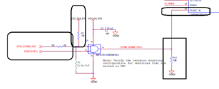
The TI E2E™ design support forums will undergo maintenance from July 11 to July 13. If you need design support during this time, open a new support request with our customer support center.

[FAQ] AM625 / AM623 / AM620-Q1 / AM62Ax / AM62Px / AM62D-Q1 / AM62L Design Recommendations / Commonly Observed Design Errors during Custom board hardware design – SK Schematics updates for Design Update Note

Other Parts Discussed in Thread: SK-AM62B, SK-AM62B-P1, SK-AM62-LP, SK-AM62-SIP, SK-AM62A-LP, SK-AM62P-LP, TMDS62LEVM, AM62L, SK-AM64B, AM6421, AM6411, SYSCONFIG, TPS65224, SK-AM62, AM3358, AM3354, AM2432, ISO7741, AM62P5-Q1, AM62P, AM62A3-Q1, AM623

Hi TI Experts,

I am referring the collaterals for the below SKs. 

SK-AM62B (PROC114A), SK-AM62B-P1 (PROC142A), SK-AM62-LP (PROC124E2A), SK-AM62-SIP (PROC162E1),  SK-AM62A-LP (PROC135A), SK-AM62P-LP (PROC164E1.1), TMDS62LEVM (PROC181E1-1)

Is there any Update to be Done on the collaterals to reuse in my custom design.

  • Hi Board designers, 

    Here are some recommended updates based on the learnings for performance improvements.

    Schematics - Design Value Updates 

    I2C pullup is recommended irrespective of IO usage for MCU_I2C0 and WKUP_I2C0

    AM62x, AM62L, AM62Ax and AM62Px processor families (I2C0 and MCU_I2C0 for AM642/AM243x)

    MCU_I2C0 - Pullup and RC added for slew rate control when pulled to 3.3V

    WKUP_I2C0 - Pullup and RC added for slew rate control when pulled to 3.3V

    Note: The below diagram is for AM64x and the same can be used for AM62x, AM62L, AM62Ax and AM62Px processor families

    These I2C interfaces are Open drain type IOs. These I2C interfaces are fail-safe IO terminals.

    The rise and fall times of the I2C signals connected to these ports must not exceed a slew rate of 0.08 V/ns (or 8E+7 V/s). This limit is more restrictive than the minimum fall time limits defined in the I2C specification. Therefore, it may be necessary to add additional capacitance to the I2C signals to slow the rise and fall times such that they do not exceed a slew rate of 0.08 V/ns.

    Refer below 


    SOC VMON_VSYS voltage monitor implementation 

    eMMC attached device supply decap

    Add decaps as required to the eMMC memory supply rails 

    eMMC interface pulls for AM62x, AM62A and AM62D that implements soft (IOs support alternate function) eMMC PHY 

    eMMC interface pulls for AM64x and AM62Px  that implements hard (IOs do not support alternate function) eMMC PHY 

    Please refer to the errata.

    https://www.ti.com/lit/er/sprz574a/sprz574a.pdf

    i2458 MMCHS: eMMC HS400 tDCD timing marginal to JEDEC spec

    USB VBUS divider 

    USB interface Provision to Bypass CMC

    USB power switch 

    Use power switch with OC indication. Connect the OC output of the power switch to SoC input

    Caution with EPHY 1V and VPP 1.8V LDO

    Miniature DQN package used.

    Package Outline

    PCB pads 

    There is a likely chance of assembly error due to the LOD outline, pins orientation and  the land pattern (pads and pitch)

    Regards,

    Sreenivasa

  • Hi Board designers, 

    Refer below workarounds when load switch is not used for resetting the SD card power supply and the supply is fixed to 3.3V

    https://software-dl.ti.com/processor-sdk-linux/esd/AM62X/09_02_01_09/exports/docs/linux/Foundational_Components/Kernel/Kernel_Drivers/Storage/MMC-SD.html?highlight=mmc#steps-for-working-around-sd-card-issues

    https://software-dl.ti.com/processor-sdk-linux/esd/AM64X/latest/exports/docs/linux/Foundational_Components/Kernel/Kernel_Drivers/Storage/MMC-SD.html


    Given below are the list of various workarounds that can be done in the device tree node to get SD card working. The workarounds are ordered in increasing order of reducing performance.

    All the changes mentioned below, are to be done in the MMCSD device tree node corresponding to the SD instance. This is usually the first (index starting from zero) instance.

    1. Restricting to a given speed mode
      • By default the kernel driver tries to enumerate a SD card in the highest supported speed mode. Given below is the order in which the driver tries to enumerate a SD card
        • SDR104
        • DDR50
        • SDR50
        • SD HS
        • SD legacy
      • These speed capabilites can be masked using device tree property sdhci-caps-mask.
        • Limit to DDR50: sdhci-caps-mask= <0x00000002 0x00000000>
        • Limit to SDR50: sdhci-caps-mask= <0x00000006 0x00000000>
        • Limit to SD HS: sdhci-caps-mask= <0x00000007 0x00000000>
        • Limit to SD legacy: sdhci-caps-mask= <0x00000007 0x00200000>

    ·   &sdhci1 {·       /* SD/MMC */·      vmmc-supply = <&vdd_mmc1>;·      vqmmc-supply = <&vdd_sd_dv>;·      pinctrl-names = "default";·      pinctrl-0 = <&main_mmc1_pins_default>;·      ti,driver-strength-ohm = <50>;·      disable-wp;·      sdhci-caps-mask = <0x00000006 0x00000000>; /* Limiting to SDR50 speed mode */·   };

    • Limiting to SD HS speed mode can also be done by using the property no-1-8-v. This disable switching to 1.8V which is required for UHS speed modes(SDR104, DDR50, SDR50)

    ·   &sdhci1 {·       /* SD/MMC */·       vmmc-supply = <&vdd_mmc1>;·       vqmmc-supply = <&vdd_sd_dv>;·       pinctrl-names = "default";·       pinctrl-0 = <&main_mmc1_pins_default>;·       ti,driver-strength-ohm = <50>;·       disable-wp;·       no-1-8-v; /* disabling all the UHS modes */};

    FAQ reference

    The below FAQ could be followed to configure the SD interface IO voltage to 3.3V only (No UHS-I support)

    https://e2e.ti.com/support/processors-group/processors/f/processors-forum/1413596/sk-am62p-lp-how-to-set-sd-card-to-3-3v-only-low-speed

    Regards,

    Sreenivasa

  • Hi Board designers, 

    Here are some guidelines that needs to be considered when selecting or designing the SOC power architecture

    • Power supplies are configured to the required voltage level and are supplies are within the ROC
    • Power architecture follows the power-up and power-down sequence as specified in the SOC data sheet
    • Power architecture meets the slew rate requirements as specified in the SOC data sheet
    • Ensure all the power supplies are available before the MCU_PORz is released
    • Monitoring of all the supply rails
    • Ensure the supplies are turned ON only after the voltage is below 0.3V (no residual voltage) after a power cycle
    • The delay between the power supply ramp and the MCU_PORz high is as per the data sheet recommendations (9.5 ms min)
    • The MCU_PORz slew is as minimum as possible to avoid internal reset circuit glitch

    Cap_VDDSx
    A capacitance in the range 0.8..1.5uF is recommended for the LDO for stability.
    This does not include the change in capacitance due to DC bias effect, temperature and ageing.


    FET switch for connecting supplies to SOC including VPP supply for eFuse
    The SOC IO supplies have slew rate requirements specified.
    Refer Power Supply Slew Rate Requirement section of the data sheet.
    The VPP supply has a 400 mA load transient current specifiec. the VPP supply is expected to be within the ROC
    during programming. FET switch or Load switch supply could dip during power-up and affect the key writing or the SOC operation

    Regards,

    Sreenivasa

  • Hi Board designers, 

    To implement UHS-I refer below steps:

    The SD card interface pullups have to be connected to the 3.3V_1.8V VDDSHV_SDIO switched supply output from the PMIC or discrete LDO or integrated LDO

    Discrete LDO

    The SD card needs to be powered using a fixed 3.3V supply.

    The 3.3V supply to the SD card needs to be switched through a power switch

    Provision to reset the power switch using SOC IOs is recommended 

    Processor IO supply sequencing

    VCC_3V3_SYS LOAD SWITCH

    SoC IO supply rails have slew rate requirements specified.

    Refer Power Supply Slew Rate Requirement section of the data sheet.

    Add a cap 220 pF or higher on the Load switch CT (Switch slew rate control) pin.

    An ANDing logic is recommend to reset the SD cars power switch. 

    The SOC VDDSHV5 supply needs to be connected to the .3V_1.8V VDDSHV_SDIO switched supply output from the PMIC

    Integrated LDO 

    AM64x EVM

    AM64x SK 

    On the SK-AM64B there are 2 options to power the VDDSHV5. Using integrated LDO (AM64x supports integrated LDO) or use PMIC LDO output.

    The SK is configured to use the integrated LDO and the PMIC LDO output is not connected.

     It is OK to connect VDDSHV5 supply to any of the 2 supply sources.

    i'm refering the data sheet(www.ti.com/.../am6421.pdf) chapter5.4 Pin Connectivity Requirements.

    There is no information for MMC1 at there. How each MMC1 pins should be treated when MMC1 is unused?

    All of the pins associated with the MMC1 port default to an off state, so you do not need to do anything to them if not being used.

    See the highlighted portion of the following note, which can be found below the Pin Connectivity table.

    Internal pull resistors are weak and may not source enough current to maintain a valid logic level for some operating conditions. This can be the case when connected to components with leakage to the opposite logic level, or when external noise sources couple to signal traces attached to balls which are only pulled to a valid logic level by the internal resistor. Therefore, external pull resistors are recommended to hold a valid logic level on balls with external connections.

    Many of the device IOs are turned off by default and external pull resistors may be required to hold inputs of any attached device in a valid logic state until software initializes the respective IOs. The state of configurable device IOs are defined in the BALL STATE DURING RESET RX/TX/PULL and BALL STATE AFTER RESET RX/TX/PULL columns of the Pin Attributes table. Any IO with its input buffer (RX) turned off is allowed to float without damaging the device. However, any IO with its input buffer (RX) turned on shall never be allowed to float to any potential between VILSS and VIHSS. The input buffer can enter a high-current state which could damage the IO cell if allowed to float between these levels.

    Start-up issue due to SD card power switch 

    https://e2e.ti.com/support/processors-group/processors/f/processors-forum/1318441/faq-am625-am623-am62a-design-recommendations-commonly-observed-errors-during-custom-board-hardware-design-sk-schematics-updates-for-design-update-note

    Note:

    It is not possible for AM64x or AM62Px because SD Cards begin operation at 3.3V and the MMC0 port on these devices is limited to 1.8V.  

    We do not expect SD Cards to be connected to the MMC0 port of AM62x, AM62Ax, AM62Dx, or AM62Lx.  SD Cards should be connected to MMC1 or MMC2 of these devices.  However, we do allow SDIO embedded devices to be connected to the MMC0 port of these devices.

    AM6411 & SDIO Impedance recommendation

    The IOs associated with the AM64x MMC1 port has nominal source impedance of 40 ohms. This should have been reflected in the AM64x IBIS model.

    The best way to determine optimum PCB traces impedance is to use the IBIS model from AM64x and the attached device in signal quality simulations. These simulations could be used to determine which specific PCB implementation provides adequate signal quality and signal rise/fall times (slew rate). I'm not an IBIS model expert, but fairly sure there is a model for each valid IO operating voltage. Let me know if that is not the case and I will assign this thread to our IBIS model expert.

    The IBIS model is the only way we define IO output characteristics.

    There are two options for changing the operating frequency of the MMC1 port. The MMCSD1 host controller has internal clock dividers that can be used to reduce the clock frequency of the MMC1 port, but these clock dividers may not provide much resolution in frequency changes. The other option would be to reduce the MMCSD1 function clock frequency, which may impact other subsystems that share the same clock domain inside the device. You may want to use the Clock Tree tool function in the SYSCONFIG tool to understand the internal clock structure of the AM64x device.

    Regards,

    Sreenivasa

  • Hi Board designers, 

    Implementation of ANDing logic for attached device reset

    eMMC

    EPHY

    Regards,

    Sreenivasa

  • Hi Board designers, 

    Connection of nRSTOUT of PMIC directly to MCU_PORz

     We define a minimum slew rate in the SOC datasheet for inputs and this creates a maximum rise time requirement. The rise/fall time for the reset signal must be less than 1000ns, not greater than 1000ns. To ensure your design meets this requirement, you may need to use a buffer between the PMIC and SOC or select a pull-up resistor value that is strong enough to charge your PCB parasitic capacitance and the SOC input capacitance in less than 1000ns. A rise significantly faster than 1000ns is preferred to minimize the potential of noise coupling to the reset signal.

    There can be long-term reliability issues associate with the input buffer if the applied signal spends too much time in the voltage region between VIHSS and VILSS. The maximum transition time allowed is 1000ns. I recommend driving the reset input with a push-pull buffer that produces a signal transition rate that is faster than 5ns to eliminate the risk of noise coupling into the signal as it transitions through the input buffer switching threshold

    I forgot to mention another important point about the MCU_PORz input slew rate. It is very easy for noise to couple on slow rising signals such that it creates non-monotonic transitions. Your MCU_PORz reset source needs to be monotonic to prevent the chance of creating glitches on internal reset as it transitions through the input buffer switching threshold. A faster slew rate on the MCU_PORz will increase your system noise immunity. The min slew rate defined in the AM62Ax datasheet is acceptable to the AM62A device but may not be acceptable for your system noise immunity requirements.

    We get request from schematic review team to add a buffer between PMIC TPS65224 RSTOUT pin and SOC MCU_PORZ pin. I think the reason is that the SOC MCU_PORZ will require the rising edge and falling edge

    The MCU_PORz is the main cold reset input for the SOC.

    The PMIC nRSTOUT is a open drain slow ramp output from the PMIC.

    When a slow ramp reset input is applies to the MCU_PORz there are likely chances that the internal reset circuit could glitch.

    A discrete push pull output buffer is recommended to minimze the slew.

    We do not have a spec for the MCU_PORz. The recommendation is faster the better. (<10ns)

    (+) [FAQ] AM623: MCU_PORz input slew rate - Processors forum - Processors - TI E2E support forums

    Implementation of MCU_PORz discrete buffer 

    Regards,

    Sreenivasa

  • Hi Board designers, 

    Cap_VDDSx voltage rating 

    Regards,

    Sreenivasa

  • Hi Board designers, 

    PMIC capacitor and feedback recommendations

    PMIC - feed back and jumper or 0R provisioning 

    Regards,

    Sreenivasa

  • Hi Board designers, 

    OSPI pullup, pulldown and series resistor implementation.

    AM62L OSPI0 interface connected to x2 memory devices

    Regards,

    Sreenivasa

  • Hi Board designers, 

    Ethernet interface (MAC) 

    Ethernet PHY EPHY reset recommendations

    Option 1 

    Option 2 

    EPHY clocking

    AM64x

    AM62x

    (27) [FAQ] AM625 / AM623 / AM620-Q1 / AM625-Q1 / AM625SIP: Ethernet PHY RGMII synchronous clock - Processors forum - Processors - TI E2E support forums

    (+) [FAQ] AM6442, AM6441, AM6422, AM6421, AM6412, AM6411 and AM2434, AM2432, AM2431 (ALV, ALX) Custom board hardware design - Ethernet - Processors forum - Processors - TI E2E support forums

    (27) [FAQ] AM625 / AM623 / AM620-Q1 / AM62Ax / AM62Px / AM62D-Q1 / AM62L / AM64x / AM243x Design Recommendations / Custom board hardware design - Queries related to RGMII interface and RGMII TI EPHY - Processors forum - Processors - TI E2E support forums

    [FAQ] AM625 / AM623 / AM620-Q1 / AM62Ax / AM62Px / AM62D-Q1 / AM62L / AM64x / AM243x Design Recommendations / Custom board hardware design - Queries related to RMII interface and RMII TI EPHY - Processors forum - Processors - TI E2E support forums

    (28) SK-AM64: clock sync - Processors forum - Processors - TI E2E support forums

    we are currently evaluating AM64xx on the SK-AM64: is there an easy way to use the 25MHz system clock via a CLKOUT pin for external peripherals
    to be brought out and used without changing various PLL clocks / multiplexers and dividers via registers?

    Basically to have 3x GPIO as CLOKOUT sync'd ( I'm looking for a solution to feed up to 3x external Ethernet PHYs with 25MHz ).

    OBSCLK0 is the only AM64x clock signal that is not generated from one of the internal PLLs. However, this clock output is only multiplexed to one pin. Software would need to configure the pin multiplexer to select this function and there is no way to prevent the attached device from seeing a short clock since the mux mode change is not synchronized to the clock output. This clock output is only provided as an observation clock.

    Your customer should consider the approach implemented on the AM64x EVM, where an external LVCMOS clock source is used as the system reference clock and distributed to multiple devices. Note: This approach requires a single input to multiple output buffer so each device receives its clock from a dedicated clock output with point to point connectivity. Any attempt to clock multiple devices from a common clock output is likely to be problematic.

    Regards,

    Sreenivasa

  • Hi Board designers, 

    AM62L RTC only Discrete LDO implementation 

    Regards,

    Sreenivasa

  • Hi Board designers, 

    Refer below for DDR4 clock termination.


    I have a question from my customer for DDR CLK termination specfication.
    According to SK-AM62 schematics (PROC114E3_SCH.pdf), page#16.
    DDR_CLKP/N are terminated by resisters and capacitor.

    Do you have DDR termination specification? How these resisters and capacitor values are defined?

    This is actually taken from the DDR4 recommendation from Micron, in their appnote TN-40-40.  Here is the quote from the appnote:

    • If simulations determine that AC termination is needed, terminate CK_t and CK_c through approximately 36Ω series resistors and a .01uF capacitor to VDD. A single approximately 36Ω resistor in parallel across CK_t and CK_c may also be adequate.

      Regards,

      Sreenivasa

  • Hi Board designers, 

    Refer below for description about SPI signal series resistor

    In 2.7 System issues of AM64x Schematic Review Checklist.pdf
    It says [Put 22-Ω series resistors (close to processor) on the output clocks of the SPI module.], but what are the acceptable tolerances?
    Is it possible to use a value such as 33Ω instead of 22Ω?

    A value of 33 ohms may actually be better than 22 ohms. The most important thing is placing the resistor close to the AM64x device to minimize the signal trace length that connect the series resistor to the AM64x pin. This is required because the SPI clock pin is operating as input and output at the same time, where the internal data capture clock is looped back in the AM64x IO buffer. This is done to help with timing closure of SPI by inserted an equivalent delay in the looped back clock as the returned data path sees with the delay inserted by the clock output buffer and data input buffer. However, this approach impacts signal integrity at the looped back clock pin.

    The help explain this issue, lets assume the output impedance is equal to the trace impedance. In this case the source end of the signal trace will only transition to mid-supply initially when the clock toggles. The signal will propagate the far end of the signal trace where it encounters a high-impedance mismatch which causes an equivalent amplitude reflection that returns to the source. For the time it take for the signal to propagate down and back, the voltage applied to the source pin will remain mid-supply. This is very likely to create glitches on the clock being looped back into the SPI controller. These glitches may over-clock the state machine and cause unpredictable operation. Adding a series resistor allows the voltage to step beyond the switching threshold, which prevents glitches. A 33 ohm will allow the voltage to step further away from the switching threshold than the 22 ohm. Increasing the resistor too much will compromise clock transition time, which may impact performance. I would avoid going higher than 33 ohms unless you observe an issue where the step function on the signal is causing problems.

    The signal trace that connects between the pin and resistor will create a similar step and this is unavoidable. However, the step will be filtered by the input buffer if short. This is why it is important to keep this trace short.

    Hopefully, this explains why we require these resistors and why they need to be close to the source pin 

    Thank you for your answer.

    I understand that it is important to make sure that:

    -Wire the SPI_CLK signal as short as possible.

    -Place a resistor of about 22 to 33Ω in series and measure the actual waveform to check if there is glitch or overshoot in the clock waveform.

    In addition, noise radiation from this CLK line is currently our problem.

    Is there any reduction method other than the following?

    -Shorten the CLK line.

    -Dull CLK by inserting a resistor or a capacitor on the order of pF.

    -Lower the impedance of the power supply and signal ground.

    Regards,

    Sreenivasa

  • Hi Board designers, 

    Refer below for description about SPI signal series resistor use case (for understanding and can be applied for AM6x)

    https://e2e.ti.com/support/processors-group/processors/f/processors-forum/1127775/am3358-a-ringing-problem-of-emmc-interface/4191109?tisearch=e2e-sitesearch&keymatch=userdisplayname%2525253A%25252522Peaves%25252522%25252520%25252526%25252526%25252520series%25252520resistor#4191109

    AM3358: A ringing problem of eMMC interface

    I do not think the voltage change observed on the clock signal while it is high is causing your problem. It appears you are probing the clock signal near the eMMC device based on the shape of the clock signal rise/fall edges. You need to probe the clock signal near the processor. I suspect you will see a non-monotonic transition near mid-supply on the source end of the PCB trace. This non-monotonic transition is likely causing the problem.

    The processor sources the clock out to the eMMC device and loops in back at the processor pin to improve timing margin. So there is a good chance the non-monotonic transition occurring at the source is creating a glitch on the clock that is looped back into the processor.

    The AM335x schematic checklist tells you to install a 33 Ω series resistor on MMCx_CLK (as close to the processor as possible). I do not see this resistor in your schematic. This resistor is necessary to prevent this problem.

    The capacitor is likely changing the signal distortion enough to make it work better, but it is not a good solution.

    The resistor doesn't eliminate the non-monotonic transition. It shifts the voltage away from the input buffer switching threshold voltage, where it is less likely to create a glitch on the looped back clock going back into the processor. The only way to resolve the clock glitch issue is install a 33 ohm series termination resistor located very close to the AM335x pin. The trace length between the processor pin and the series resistor should be as short as possible. 

    AM3354: MMC clock timing

    https://e2e.ti.com/support/processors-group/processors/f/processors-forum/1037185/am3354-mmc-clock-timing/3846519?tisearch=e2e-sitesearch&keymatch=userdisplayname%253A%2522Peaves%2522%2520%2526%2526%2520series%2520resistor#3846519

    I did not see any de-coupling capacitors between on the AM335x VDDSHV4 power pin after low pass filter L704. Were these accidently omitted in the snapshots provided? If not, each power pin needs local de-coupling capacitors after their respective low pass filters.

    I’m concern with the SD Card ground connections. Hopefully the SD Card VSS1 and VSS2 pins are connected directly to the same ground as the AM335x device. I assume the other grounds shown for the SD Card are simply the metal chassis ground and they are not part of the SD Card signal and power ground connections.

    They should not be using a zero ohm resistor for R514. This should be a 22 - 50 ohm resistor. The MMC/SD host controller in AM335x loops the clock back at the pin to improve timing margin for the internal circuits. However, there is a negative side effect of implementing clock loopback on a pin. The clock signal will be distorted on the source end of a signal trace and a series resistor of 22 - 50 ohms is required to modify the signal distortion such that is does not create a glitch on the looped back clock signal.

    I will explain what happens. The clock output buffer inside AM335x has a source impedance of about 30- 50 ohms and a typical PCB signal trace has a characteristic impedance in the range of 40 - 60 ohms. When the output buffer toggles the signal from low to high or high to low, the voltage of the pin which sits between the output buffer and the PCB signal trace will not transition to the expected voltage immediately. This is because the output buffer impedance and trace impedance create voltage divider that causes the pin to step to a mid-supply voltage for a short time. This step will last as long as it takes for the clock signal to travel down the PCB signal trace to the SD Card, where it encounters a high impedance load that creates a reflection that allow the voltage  to increase to VDD or VSS. The amplitude of the mid-supply voltage step may be near the AM335x clock buffer input switching threshold, which allows noise to create a glitch on the AM335x internal clock. The series resistor raises the impedance of the PCB portion of the voltage divider such that the voltage at the pin steps above or below the switching threshold.

    I suspect this is what is causing the instability and the reduced clock amplitude is contributing to the issue.

    What you observe on this signal depends on where you connected the probe, the bandwidth of your probe/scope, and quality of your scope probe ground. 

    You will need a very high bandwidth probe and scope to observe short over-shoot, under-shoot, and non-monotonic events on the signal. I recommend using a low capacitance FET probe with a very-very short low loop inductance ground.

    You will see a mid-supply step on the signal when probing near the source. This occurs because the output impedance of the MMC0_CLK output buffer, series termination resistor, and characteristic impedance of the PCB signal trace creates a voltage divider. The voltage divider output is applied to the source end of the PCB signal trace. This voltage propagates down the trace to the far end where it encounters a high impedance load which causes a in-phase reflection that returns to the source. Therefore, the voltage transition observed on the far end will be a continuous transition between VSS and VDD. The is not the case for the source end, as it steps to a mid-supply determined by the voltage divider values and the transition only continues to VDD or VSS once the reflection returns from the far end. You need to select a series resistor value that allows the MMC0_CLK pin to step through the voltage of (VDDSHV4 / 2) without pause. I suggest the step observed on the MMC0_CLK pin should be at least 200mv above (VDDSHV4 / 2) on the rising edge and at least 200mv below (VDDSHV4 / 2) on the falling edge.

    Regards,

    Sreenivasa

  • Hi Board designers, 

    Refer below for description about SPI

    SPI_MISO_ voltage was dropped from 3.3V to 2V
    Query
    Customer connected ADC data output (MISO) to AM2432 through ISO7741 using SPI interface. The expected voltage level of SPI_MISO_ADC was 3.3V, however it dropped down to 2V.
    Answer
    I can only assume their software has configured pin A14 on the AM243x device as an output and it is in contention with the output of the ISO7741 device.
    Have customer check the voltage of this signal while the AM243x is held in reset?
    Have customer disable the AM243x output buffer by writing the appropriate value to the TXDIS bit in the respective PADCONFIG register during this condition to see if the signal voltage changes.
    Result
    Customer disabled TX_DIS then voltage level became normal.

    Regards,

    Sreenivasa

  • Hi Board designers, 

    Information related to clock pulldown 

    e2e.ti.com/.../faq-am625-what-s-the-purpose-for-the-pull-down-r-on-mmc_clk

    May I know what the purpose for the pull down R on MMC_CLK signal on TI EVM? May I know what the purpose for the pull down R on MMC_CLK signal on TI EVM? 
    Most of the IOs associated with the AM62x device default to the off state, which means any attached device input without an internal pull resistor would be floating until software configures the pin to drive the signal. We use an external pull-down rather than an external pull-up since the clock signal is held in a low logic state when paused.

     Because there are cases where the clock is stopped or paused in a low logic state and the pull-down option is consistent with this logic state.

    Regards,

    Sreenivasa

  • Hi Board designers, 

    Information related to clock measurement

    What you observe on this signal depends on where you connected the probe, the bandwidth of your probe/scope, and quality of your scope probe ground. 

    You will need a very high bandwidth probe and scope to observe short over-shoot, under-shoot, and non-monotonic events on the signal. I recommend using a low capacitance FET probe with a very-very short low loop inductance ground.

    You will see a mid-supply step on the signal when probing near the source. This occurs because the output impedance of the MMC0_CLK output buffer, series termination resistor, and characteristic impedance of the PCB signal trace creates a voltage divider. The voltage divider output is applied to the source end of the PCB signal trace. This voltage propagates down the trace to the far end where it encounters a high impedance load which causes a in-phase reflection that returns to the source. Therefore, the voltage transition observed on the far end will be a continuous transition between VSS and VDD. The is not the case for the source end, as it steps to a mid-supply determined by the voltage divider values and the transition only continues to VDD or VSS once the reflection returns from the far end. You need to select a series resistor value that allows the MMC0_CLK pin to step through the voltage of (VDDSHV4 / 2) without pause. I suggest the step observed on the MMC0_CLK pin should be at least 200mv above (VDDSHV4 / 2) on the rising edge and at least 200mv below (VDDSHV4 / 2) on the falling edge.

    Regards,

    Sreenivasa

  • Hi Board designers, 

    Information regarding power supply sizing:

    The recommendation is to take into account the maximum current rating (provided in the Maximum Current Ratings application note) for power  supply sizing

     PET tool could be used for doing power estimation for an use case.

    Regards,

    Sreenivasa

  • Hi Board Designers, 

    Refer below inputs regarding SD card power switch reset logic implementation:

    AM62P5-Q1: RESETSTAT and PORz_OUT for SD card power enable. 

    Customer is considering to adopt AM62P for their system. Then they are confirming the schematic of AM62P.

    In the schematic of AM62P EVM, RESETSTATz and PORz_OUT are ANDed to the SD Card power enable signal.

    Customer also understand that RESETSTATz is also asserted when PORz_OUT is asserted.

    Is this understanding, correct?

    Is the circuit like this because the timing is slightly different when asserting?

    In that case, please tell us what the timing between RESETSTATz and PORz_OUT.


     The system power on reset is connected to ensure the card power is forced off as soon as power is applied since this reset is expected to be valid while power supplies ramp.  The RESETSTATz is included so the SD Card is power cycled (Reset) if there is a processor warm reset source like a watchdog time-out. The GPIO is connected to allow the software driver to reset (cycle power) the SD Card.

    The RESETSTATz will not be valid until all AM62Px power rails are valid, so it is delayed relative to the system power on reset.

    Regards,

    Sreenivasa

  • Hi Board Designers, 

    Refer below inputs regarding SD card SDCD pin

    AM62A3-Q1: SDCD Interface

    The SDCD signal function associated with the MMC1 port is part of the VDDSHV0 IO power domain, so this signal must operate from the same power supply that is sourcing VDDSHV0.

    The SDCD signal function associated with the MMC2 port has three pin multiplexing options, where two are part of the VDDSHV0 power domain and the other is part of the VDDSHV6 power domain. The operating voltage of this signal must be from the same source being used to power the respective IO (VDDSHV0 or VDDSHV6 power domain).

    I do not understand why this is a concern. Normally the SDCD signal is only connected to switch on the SD Card slot, where the signal is pulled high with a pull-up connected to the same power rail that is powering the associated IO and the switch in the SD Card slot will pull the signal to VSS when a card is inserted. The switch doesn't care what voltage is applied to the pull-up.

    The SDCD and SDWP signal functions are defined by industry specifications. It is important not to confuse the physical layer signal requirements with the IP register definitions. 

    Signal/Physical Layer Definitions:

    Card Detect (MMC1_SDCD)

    0 (Logic Low - VSS) = Card Detected

    1 (Logic High - VDD) = No Card Detected

    Write Protect (MMC1_SDWP)

    0 (Logic Low - VSS) = Write Protection Disabled (Write Enabled)

    1 (Logic High - VDD) = Write Protection Enabled (Write Disabled)

    The IP registers and associated bitfield definitions are not necessarily required to exactly reflect the logical truth table defined by the physical layer specification.

    AM623: uSD Card Detection Without Card Detect

    https://e2e.ti.com/support/processors-group/processors/f/processors-forum/1380597/am623-usd-card-detection-without-card-detect

    Ok but since the uSD Card Carrier does not have provision for Card Detect switch, the customer would hard wire it to 0.  Then what happens to my 2 use cases? especially if no uSD is present?

    the ROM will attempt to boot if the card detect is sampled active low.  If it doesn't find an image (which it won't if no card is detected), it will timeout and move on to the secondary boot source.

    https://e2e.ti.com/support/processors-group/processors/f/processors-forum/1073906/am6442-sd-card-decection-without-card-detect-pin

    The ROM code team has confirmed they check the card detect input and will not boot from the SD Card if a card is not detected. Therefore, your product needs to use a SD Card connector with a card detect switch to properly indicate when a card is inserted in the connector.

    https://e2e.ti.com/support/processors-group/processors/f/processors-forum/1294930/faq-am6442-am6442-sd-card-interface

    This power switch, along with the reset logic, and the host IO power supply circuit is required to support UHS-I SD Cards which begins communications using 3.3V signal levels and later change to 1.8V signal levels when changing to one of the faster data transfer speeds. Cycling power to the SD Card is the only way to put it back into 3.3V mode since SD Cards do not have a reset pin. The host IO power supply must power off/on and change voltage at the same time as the SD Card. These circuits and the software driver operating the signals sourcing these circuits ensure both devices are off, or on and operating at the same IO voltage at the same time. 

    https://e2e.ti.com/support/processors-group/processors/f/processors-forum/1027630/tda4vm-mmc_sdcd-not-connected/3799072

    We have a custom board based on a TDA4x SoC and have trouble booting from the SD card.

    We noticed the MMC1_SDCD pin (card detect) but our MicroSD socket doesn't have this functionality (card detect switch).

    Is it possible to skip SDCD checking from TDA4x side?

    Is there a way to set BOOTMODE pins differently to change this MMC1_SDCD impact?

    If booting from MMC1, the SDCD pin is required to be low to indicated card is available.  The pin can be tied low or connected to card detect from card cage.  This is required from MMC1 boot process with no bypass mechanism.

    https://e2e.ti.com/support/processors-group/processors/f/processors-forum/1115074/faq-am625-mmc-interface

    • The boot code in AM62x only supports booting from an CD Card on MMC1.

      MMC1_SDCD and MMC1_SDWP pins are powered from the VDDSHV0 power domain. So they must operate at a fixed voltage that is the same for all IOs associated with VDDSHV0. Each of these signals should have an external pull-up resistor connected to the same power supply that powers VDDSHV0. They are also connected to their respective switch in the SD Card connector, where the other side of the switch is connected to ground. The operating voltage of these signals is completely independent of the SD Card IO operating voltage since these signal do not connect to the SD Card. They do not need to change their operating voltage like the other MMC1 signals when using one of the higher speed data transfer modes supported by UHS-1 SD Cards.

    • Regarding the SD card power rail, if we  locked the power rail “VDDSHV0” to be 1V8, is there any risk besides we only use the ultrahigh speed SD card

    • The only pins associated with MMC1 that are powered from VDDSHV0 are MMC1_SDCD and MMC1_SDWP.  These pins are not connected to the SD Card. They only connect to switches in the SD Card connector and should be pulled high with an external resistor connected to the same supply that is powering VDDSHV0. The other side of the switches in the SD Card connector are connected to ground to indicate a card is present or the write protect switch is on.

      All of other MMC1 pins are powered from VDDSHV5. These pins are connected to the SD Card, where they are required to begin communications with the SD Card using 3.3V and only change to 1.8V after the host negotiates a voltage change with the card. This is the way SD Cards work to ensure they are backwards compatible with older systems.  So your VDDSHV5 supply must always default to 3.3V when power is applied and designed to change from 3.3V to 1.8V when software is ready to change the operating voltage of these pins. The SD Card is always powered from a switched 3.3V supply since it has internal circuits that switches its IO voltage at the same time. Note: the SD Card must have a software controlled 3.3V load switch that allows power to be cycled since this is the only way to reset the card and place it back into its default state.

      You may need to read the SD Card standard to understand all of the details required to implement a system that supports the more complicated UHS-1 cards.

    Regards,

    Sreenivasa