This thread has been locked.

If you have a related question, please click the "Ask a related question" button in the top right corner. The newly created question will be automatically linked to this question.

IWR6843AOP: Query on Sensing Performance and Simulation for IWR6843AOP in Custom PCB Design

Part Number: IWR6843AOP
Other Parts Discussed in Thread: , DCA1000EVM, MMWAVE-STUDIO

Tool/software:

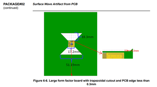
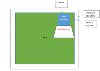
Query 1: When designing the mmWave radar's PCB for our product, our initial approach is to replicate the evaluation board's design IWR6843AOPEVM on our PCB to minimize any deviations or influences caused by design changes. However, if space constraints arise—such as positioning the mmWave radar IC (IWR6843AOP) at the center of the product what impact could this positional change (e.g., moving the IC IWR6843AOP to the center or corner relative to the evaluation board design) have on the radar's sensing performance?

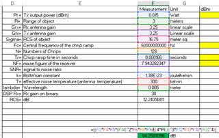
Query 2: Is there a method to simulate the IWR6843AOP module's sensing performance within the product's enclosure to evaluate potential impacts?

Query 3: what are the possible most compulsory test we need to perform at the production line for the mmWave radar IWR6843AOPEVM.

Query 4: ETSI EN 305-550-1 suggested on your website states that device “Must be able to turn off the radar if other radar devices are nearby”. Is this feature available in TI’s RADAR chip? (dev.ti.com/.../node

Query 5: Is 60GHz-64GHz frequency band allowed in India and UK for in-house commercial use applications?

Query 6: is there any way to simulate IWR6843AOP antenna performance? 

  • Hi,

    We are looking into your query. Please allow us a couple of days to respond.

    Regards,

    Sharan

  • Hi Dileep,

    Please find below my responses:

    1.  

    When designing the mmWave radar's PCB for our product, our initial approach is to replicate the evaluation board's design IWR6843AOPEVM on our PCB to minimize any deviations or influences caused by design changes. However, if space constraints arise—such as positioning the mmWave radar IC (IWR6843AOP) at the center of the product what impact could this positional change (e.g., moving the IC IWR6843AOP to the center or corner relative to the evaluation board design) have on the radar's sensing performance?

    Please refer to the IWR6843AOP device errata advisory number PACKAGE#02: Surface Wave Artefact from PCB, for guidelines about device placement.

    IWR6843AOP Device Silicon Errata 

    2.

    Is there a method to simulate the IWR6843AOP module's sensing performance within the product's enclosure to evaluate potential impacts?

    If TI EVM is followed there won't be necessity for simulations. If you still want them, please contact your local TI field team. The simulation information is available for NDA signed customers.

    3. 

    what are the possible most compulsory test we need to perform at the production line for the mmWave radar IWR6843AOPEVM.

    Please refer to mmWave Production Testing Overview application note for this query.

    4. 

    ETSI EN 305-550-1 suggested on your website states that device “Must be able to turn off the radar if other radar devices are nearby”. Is this feature available in TI’s RADAR chip? (dev.ti.com/.../node

    Yes, this feature is available in TI's radar devices.

    5.

    Is 60GHz-64GHz frequency band allowed in India and UK for in-house commercial use applications?

    In India, the regulatory guidelines keep changing. It would be best to contact local regulatory test houses to get the most recent regulations.

    For UK too, the regulations keep changing especially after the Brexit happened. Hence it would be best for UK also to contact the local test houses to get the most recent regulations.

    6.

    is there any way to simulate IWR6843AOP antenna performance? 

    Yes, there is. Please contact your local TI field team for more details on it. The simulation information is available for NDA signed customers.

    Thanks

    Swarnendu

  • Hello Swarnendu,

    As per your input, when using two IWR6843AOPEVMs in a single room or in close proximity, one of them should ideally be switched off to avoid interference. However, we performed an experiment where both radars were placed on a table facing each other, and neither of them stopped working. Additionally, we installed the two modules on opposite walls of the room, directly facing each other, and both modules continued to operate without any issues. Could you please help us understand the possible reasons for this behavior?

    I also have a few additional questions:

    1. What tests should I perform to characterize the IWR6843AOP module from a hardware perspective? Possible test to control the variability on the products. 
    2. If we proceed with this module for production, how can we ensure robust quality assurance of the chip to avoid critical chip-level failures in the production line? please suggest the possible test to control the variability on the production.
    3. How can we measure the transmit power of the IWR6843AOP module in our lab? Alternatively, is there any third-party service available in India for this purpose?
  • Hi Dileep,

    I think there is a misunderstanding here. "No carrier sense required, must be able to turn off the radar if other radar devices are nearby" this statement is from regulatory perspective, and this is not an automatic feature that is available in the device. However, manually it can be activated. Algorithm needs to be developed for that.

    Regarding your questions:

    1 & 2. For production testing please refer to the application note: mmWave Production Testing Overview (Link)

    3. Transmit power can be measured using power meters in lab. TI does not work with any third-party test houses in India. Below I am listing down few Global test houses:

           Eurofin

           Nemko 

    Thanks,

    Swarnendu

  • Hello Swarnendu,

    I just need confirmation has TI implemented this on the IWR6843AOPEVM?

    Additionally, I have a few more questions:

    1. Could long-term exposure to the IWR6843AOP module be hazardous to human health? If not, is there any certification available to confirm this?
    2. Could you provide spurious emission test data for the TI mmWave IWR6843AOP module? Specifically, which limits the module has passed in relation to the required standards?
    3. How is the IWR6843AOP module calibrated on the production line? Can you share any related documentation? Also, is a different firmware required for calibration?

    Thanks & Regards,
    Dileep

  • Dileep,

    Please find on how we can address this:

    Managing interference in FMCW radar systems | Video | TI.com 

    https://www.ti.com/lit/an/swra662a/swra662a.pdf 

    Please find below my responses:

    1. Please find the necessary certificate in https://dev.ti.com/tirex/explore (mmWave radar sensors/Hardware kits and board/IWR6843AOPEVM/Emission certificates/RED Certification Collateral/EN 62311 report)

    2. Please find the necessary certificate in https://dev.ti.com/tirex/explore (mmWave radar sensors/Hardware kits and board/IWR6843AOPEVM/Emission certificates/FCC Certification Collateral/FCC 47 CFR Part 15, Subpart B Report)

    3. Please find details about self-calibration in the appnote: https://www.ti.com/lit/an/spracf4c/spracf4c.pdf 

    For your reference, please refer to xWR6843AOP hardware design checklist: https://www.ti.com/lit/zip/swrr197 

    You will find necessary information and resources in the checklist. Also, you can explore https://dev.ti.com/tirex/explore to find details on antenna radiation patterns and other details.

    Thanks,

    Swarnendu

  • Dear Swarnendu,

    Thank you very much for the information you provided earlier. It has saved me a lot of effort and time, and it has cleared almost all of my doubts.

    I have one final query: where can I find all the calculations required for designing the hardware-level blocks for the IWR6843AOPEVM?

    Thanks and regards,
    Dileep 

  • Dileep,

    The best document to refer to get guidance on the hardware design is the hardware design checklist: https://www.ti.com/lit/zip/swrr197 

    It has all the necessary information for hardware design. Please refer to different sections in the checklist. 

    Thanks,

    Swarnendu

  • Dear Swarnendu,

    As you may already know, the 60-64 GHz frequency band is not freely available in India. Therefore, we are considering using it within the ISM band (61 to 61.5 GHz), where only 500 MHz of bandwidth is available.

    I would like to understand the impact of this bandwidth limitation on performance, based on calculations or experimental results, for the following parameters:

    1. Object detection accuracy
    2. Static presence detection performance
    3. Velocity resolution
    4. Field of view
    5. People counting and tracking
    6. Maximum and minimum range for object detection
    7. Any other relevant impacts

    Looking forward to your insights.

    Thanks and regards,
    Dileep 

  • Hi Dileep,

    Bandwidth does not have direct impact over the max range, max velocity, velocity resolution, angular range or angular resolution. Field of view also depends on the antenna radiation pattern and is unaffected by chirp bandwidth.

    However, it has impact over the range resolution. With 500MHz bandwidth, the range resolution will be 30cm. Hence, it will also have some impact on static presence detection and people counting/tracking. If multiple objects stay less than 30cm apart, they will be considered as a single object.

    For a better understanding on the chirp parameters and their impact over radar performance, I would like to refer to the application note to you: 

    https://www.ti.com/lit/an/swra553a/swra553a.pdf (link)

    Please take a look on the appnote for other detailed considerations.

    Thanks,

    Swarnendu

  • Hello Swarnendu,

    I hope you're doing well.

    I have a question regarding the placement of the IWR6843AOP module on the PCB. As per the guidelines, the module should ideally be positioned to minimize surface wave reflections in the E-plane, which involves shaping the PCB into a trapezoidal cutout. However, due to space constraints on my PCB, I cannot accommodate this shape.

    Could you suggest any possible workarounds for this issue? Additionally, if I position the module at the edge of the PCB on one side, while the other side has no cutout, will this setup cause any adverse effects due to the edges of the radome or the heatsink at the back of the chip?

    Regards, 

    Dileep Sharma

  • Hi Dileep,

    I am doing well. Hope you too are doing fine.

    It is OKAY to put the AOP device close to the PCB edge on one side. In that case I would recommend having the trapezoidal cut out on the other side of the PCB. I assume the device will not have PCB edges in both the north and south sides. If cut out or PCB edge is not placed in both the sides, ripples could be observed in the antenna radiation pattern in the elevation side as depicted in the device errata.

    For radome design, please refer to the below appnote:

    https://www.ti.com/lit/an/swra705/swra705.pdf 

    Longer components should not be placed in the device side of the PCB. 

    Thanks,

    Swarnendu.

  • Hello Swarnendu,

    We are planning to place the module as shown in the image below on the PCB.

    Could you please explain the possible impact on the radiation pattern of the mmWave radar? Additionally, what would be the impact on the Field of View (FOV)? Is the above implementation correct to proceed with?

    Also, could you clarify how the trapezoidal cut distance is calculated? Lastly, what will be the impact on the FOV due to nearby components on the PCB near the radar?

    Thank you

    Dileep

  • Dileep,

    I would recommend you stick with the provided dimensions in errata for the trapezoidal cut:

    These dimensions are optimized through antenna simulations. Also, I would like to recommend the device to PCB edge distance be less than or equal to 0.3mm. This is to prevent higher order radiations as well as to prevent unwanted emissions from other PCB components affecting the antenna performance. The design you provided with one side of the device facing the PCB edge and the other having the trapezoidal cut is alright, given the cut dimensions and the device to PCB edge distances are same as what is provided in the errata.

    As an alternate workaround, as you asked, I can suggest using board to board connection. In this, the AOP device can be placed on a different board maintaining the edge to device spacings and taking out important signals out of the board to connect to the main board with other functionalities. This will help addressing area constraints.

    However, the proposed design would work fine (i.e. PCB edge at one side and trapezoidal cut out at another).

    With the recommended design, we should be able to address the surface wave artifacts. Regarding the antenna field of view, the north and south sides are anyway having no components. Considering the east and west sides, I would like to recommend placing components at least one wavelength away from the device. It is best if we can manage all other components to the other side of the PCB, but a one wavelength space is also fine.

    Thanks,

    Swarnendu

  • Hello Swarnendu,

    As per your suggestion, I have tried to create a possible design option. Please review it and share your feedback. The design details are attached below.

    In the attached images (top view and side view), I have a concern regarding the placement of the heat sink below the radar module. A thermal pad is positioned between the radar and the heat sink. Will this setup still have any impact?

    Additional one more question with reference to below image 

    Regards,

    Dileep

  • Hi Dileep,

    From the diagram you shared, I can see the radar device placed on a narrow PCB that is allowing the radar device having PCB edges in both North and South sides. I would like to ensure that device edge to PCB edge space is <= 0.3mm. Also, is this a different PCB, as based on the previous discussions we came to a point that one side the device will have PCB edge and the other side a trapezoidal cut?

    As far as I can see, the heat sink is below the radar device and not intersecting the radar device plane. In that case it is okay. Even though I would like to ensure that no component should come inside the RADAR FoV.

    For the second question, yes there could be non-conducting material. The idea of introducing a trapezoidal cut is to ensure that at least in the marked area, there should not be any PCB to provide conducting surface so that it would interact with the radar performance. Again, I would like to sensitize that any components placed in the vicinity of radar device should not affect its FoV, hence the height of these components need to be checked properly.

    Thanks,

    Swarnendu

  • Hello Swarnendu,

    This is the same PCB we discussed previously, but the issue and concern we are facing is that when we shift the PCB further toward the edge, there are some mechanical snaps. Additionally, there might be an impact due to the enclosure. When we move the PCB further north (upward), the shape of the enclosure in the FOV path changes—it is curved at the edges and flat at the center. This might impact performance.

    To address this, we are considering the design shown in the previous image I shared. In this case, there is a heat sink positioned at the back, just below the 3.2 mm gap (the PCB and thermal pad are positioned between the IWR6843AOP module and the heat sink.). Although the heat sink is not directly in the FOV, is there any possibility that it could impact performance?

    Additionally, I can adjust the PCB placement on the top, but I haven’t analyzed the impact yet. This is because two factors change in the FOV of the chip:

    1. The shape of the enclosure.

    2. The distance between the AOP module and the enclosure (Curved at edge).

    If you have any suggestions regarding this, please share.

    Lastly, space is limited in this design, and I also need to accommodate Wi-Fi. Could there be any interference issues in this setup?

    Regards, 

    Dileep 

  • Dileep,

    For the enclosure/radome design you can take a look at the below application note:

    https://www.ti.com/lit/an/swra705/swra705.pdf 

    Yes, as the heat sink lies below the device plane, it should not impact radar performance.

    Also, integrating Wi-Fi should not interfere with the radar performance.

    Thanks,

    Swarnendu. 

  • Hello Swarnendu,

    I would like to request reference documents that provide detailed information about the radiation pattern and surface wave reflection of MIMO antennas. Like how FOV is formed with MIMO antennas. 

    Additionally, I seek clarification on Field of View (FOV) calculations. Specifically, should the FOV be calculated from the edges of the module or from the center of the module?

    Regards,

    Dileep

  • Hi Dileep,

    I would like to refer the below documentations for the antenna radiation patterns:

    IWR6843AOP 

    https://www.ti.com/lit/ds/symlink/iwr6843aop.pdf (Device data sheet - Section: RF Specification)

    Regarding the surface wave artifacts, the optimized workarounds are mentioned in the device errata. Those should be well enough to deal with the same.

    FoV is determined based on the antenna radiation pattern. The considerations are keeping the radar device at center. In both azimuth and elevation sides, the field of view is -60 deg to +60 deg.

    Thanks,

    Swarnendu

  • Hello Swarnendu,

    • Can you provide the detailed power dissipation breakdown for different components of the radar (e.g., Tx, Rx, DSP, LDO, or any other components)? The datasheet provides the combined value for all sections, but I require individual values for each section.

    • What is the heat dissipation when the radar front end (e.g., Tx/Rx) is not in use or when the radar is not transmitting?

    • If I frequently turn the radar on and off to reduce heat dissipation, what will be the impact on its performance and overall system reliability?

    Thanks and Regards,

    Dileep Sharma

  • Hi Dileep,

    1. The operation of each individual subsystems such as DSP/Processing highly depends on device configurations especially sampling rate, #Chirps, duty cycle etc. Hence it is difficult to standardize power dissipation for each of these subsystems.

    2. Please refer to the application note: Thermal Design Guide for Antenna on Package mmWave Sensor (https://www.ti.com/lit/an/swra672/swra672.pdf)

    You can use below function or API – to read the junction temperature.

    mmwaveLink_getTemperatureReport()  

    rlRfGetTemperatureReport()

    3. If junction temperature is maintained below 105 deg C, below is the power on hours for the mmWave device.

    You can check using the other knobs to reduce the temperature (Such as duty-cycle, Heat-sink options etc).

    There should not be performance impact for frequent power cycles. But in longer terms it might stress out the PDN.

    Thanks,

    Swarnendu

  • Hello Swarnendu, 

    1. What is the power consumption when the radar front-end system is idle or not operational?

    2. How much power dissipation occurs in the following scenarios:

    1.  When only one Tx is active with the maximum duty cycle.
    2.  When two Tx antennas are active with the maximum duty cycle.
    3.  When all three Tx antennas are active with the maximum duty cycle.

    3. By what percentage does the performance get impacted when switching from all three antennas operating simultaneously to just one antenna at a time?

    Thanks 

    Dileep

  • Dileep,

    Please find below my responses:

    1. We do not have any comprehensive power numbers for the device idle state (i.e. front end inactive) because this is highly user specific. It depends on how many communication interfaces are active, what are the supplies to the device etc. However, the digital leakage power can be expected to be ~20mW.

    2. There are many configuration parameters that the average power dissipation depends on. Definition of max. duty cycle also varies based on different regulations. To give you an estimate I am providing below some numbers. However, these will not be exactly specific.

    2.1 Only 1 TX, High duty cycle: 1.7W

    2.2 Only 2 TX, High duty cycle: 1.9W

    2.3 All 3 TX, High duty cycle: 2.2W

    3. I am stating below the improvements you will observe if more #TXs are used:

    a) The transmitted power will be more.

    b) #Virtual antenna array will increase with each TX antenna by a multiplication of #RXs, which will increase the angular resolution.

    c) The overall noise floor will reduce.

    Similarly with lesser TXs you will observe some degradation on the said factors.

    You can further explore IWR6843AOP low power modes in the below resources:

    https://www.ti.com/lit/an/swra689/swra689.pdf?ts=1734701696344&ref_url=https%253A%252F%252Fwww.google.com%252F 

    https://dev.ti.com/tirex/explore/node?node=A__ALuG45QtveCbcI.ZvVcCOw__com.ti.mmwave_industrial_toolbox__VLyFKFf__LATEST 

    Thanks,

    Swarnendu

  • Hello Swarnendu,

    As stated in the IWR6843AOP datasheet, information on average power consumption is provided as below:

     However, the datasheet does not specify the average power consumption when all three transmitters are active. Can I get the information?

    Additionally, I have one more query when i am changing the configuration No. of TX to be used the GUI is not parsing the data does the 3d people tracing binary support the configuration of changing the No. of Tx. 

    Thanks 

    Dileep Sharma 

  • Hi Dileep,

    Please refer to the below table note (Table 8-3. Maximum Current Ratings at Power Terminals) for the simultaneous 3 transmitter use case effects on power consumption:

    There is more than one factor that could be affected for any change in the configuration. To verify the changes to examine other places that it can impact please refer to mmWave sensing estimator (mmWaveSensingEstimator).

    Thanks,

    Swarnendu

  • Hello Dileep

    Could you please guide us on how to measure the actual power consumption of the IWR6843AOPEVM when varying parameters such as active mode and idle mode optimizations?

    Additionally, we would like to know how to directly implement idle mode optimization techniques in the configuration. Any suggestions or recommendations regarding power measurement methods and configuration adjustments would be greatly appreciated.

    Thanks & regards,

    Dileep Sharma

  • Hi Dileep,

    You can measure the device level power consumption replacing the L11, L12, L13 and L14 with current sense resister. 

    TCP202 current probe can be used. For further details on measurements please refer to the application note: xWR6843 Power Optimization (https://www.ti.com/lit/an/swra689/swra689.pdf) Section 5.1 Power Measurement Method.

    For the software controls of idle power cycle please refer to the web page in TI resource explorer (68xx Low Power Demo User Guide).

    Thanks and regards,

    Swarnendu

  • Dear Swarnendu,

    How we can calculate the SNR for the corner reflector is there any excel file available for the same for the direct calculation. how to decide the NF = Noise figure of the receiver. and how to convert the dBm to dBFs. 

    and how we can test Angle Estimation Accuracy for the IWR6843AOP.

    Thanks and Regards

    Dileep Sharma 

  • Hi Dileep,

    We can calculate the RCS (Radar Cross Section) of the corner reflector and calculate the SNR using the below formula:

    Please refer to the below appnote:

    (https://www.ti.com/lit/an/swra553a/swra553a.pdf)

    Receiver EINF (effective isotropic noise figure) is 9dB. 

    dBFS is dB with respect to full scale. It is a comparative measurement unit, and it is not for absolute measurement purpose. Hence, it cannot be converted to other absolute units. dBFS is used to estimate the comparative response between different factors (for example: FFT response of radar ADC data. The purpose is to identify the peaks with respect to the noise floor. Here, absolute signal strength is not required.)

    In order to test the angle estimation accuracy, raw ADC data can be captured and post processed to get the radiation pattern by taking data all across the FoV. The angle accuracy can be determined in the post processing. You can get the reference matlab codes for post processing in the MMWAVE STUDIO download.

    Thanks,

    Swarnendu.

  • Hello Swarnendu, 

    We are in the process of simulating the mmWave radar with and without a radome. To validate the simulation, we need to replicate the results through practical experiments. Could you guide us on how to generate similar plots as shown in the images below?

    Additionally, are there detailed guidelines available to ensure that the simulation results align with the practical outcomes?

    Could you provide a detailed explanation for plotting the above graphs, including the tools, setup, and process involved?

    Thanks and Regards

    Dileep Sharma

  • Hi Dileep,

    You would require capturing the raw ADC data from the device. For this you would also need the DCA1000 capture card. The captured data can be post processed to get the plots.

    To capture raw ADC data from the device, I would like you to refer the IWR6843AOP EVM user guide (https://www.ti.com/lit/ug/swru546e/swru546e.pdf) section - 4.8.2 DCA1000EVM Mode. In this section the guidelines to connect the device to the DCA1000 is mentioned. You can connect the device as per MMWAVE-STUDIO user guide to make the set-up ready for data capture.

    I would like you to download the MMWAVE-STUDIO, from the product page (IWR6843AOP data sheet, product information and support | TI.com) in the Software development foil.

    In the MMWAVE-STUDIO download you will also find the Matlab scripts to generate these plots.

    To list it down, below are the tools you would require:

    1. DCA1000 capture card

    2. MMWAVE-STUDIO

    3. Post process scripts (Matlab)

    Also, to capture data across the azimuth and elevation FoV, additionally you would require:

    4. Corner reflector

    5. Anechoic chamber

    6. A gimbal for device rotation to cover the FoV sweep.

    Thanks,

    Swarnendu

  • Hello Swarnendu,

    Happy New Year!!

    As per your suggestion, I have attempted to collect data using the DCA1000 board and used a corner reflector with an RCS of 16.5 m², placed at a distance of 3 meters. Below are the chirp configurations I used:

     Below is the image of Post processing:

    When I am calculating the SNR by the formula you have provided, I am getting the Below output:

    However, the SNR in the two cases (from post-processing and manual calculation) does not match. Could you please suggest where I might have made a mistake? Additionally, could you prepare the calculations for the above chirp parameters in an Excel sheet for reference?

    Thank you for your time and guidance.

    Best regards,
    Dileep Sharma

  • Dear Swarnendu,

    As per your suggestion, I have collected the raw data using a turntable. However, I am facing challenges in plotting the FOV with this data. Specifically, the gain shown in the above image appears to be unusually high. Could you explain how this might be possible?

    Additionally, to obtain the FOV, do I need to calculate and plot it for each angle separately and then merge the plots? I could not find a single plot option in the post-processing menu to generate the FOV, as shown in the examples. Could you kindly point me to the exact location or file name in MATLAB that can be used to plot it?

    Thanks, and regards,

    Dileep Sharma 

  • Hi Dileep,

    Happy new year!

    Before proceeding I would like you to show us the experiment set up. the doppler plot is sensing non-zero velocities which is unusual. There should be one spike at 0-velocity. Also, the range plot should have a single spike at the expected distance the corner reflector is placed. Please also share the analog ADC plots in the studio.

    Thanks,

    Swarnendu

  • Hello Swarnendu,

    Unfortunately, I did not take setup photos. Could you please confirm if the calculations I shared with you are mathematically correct for this particular distance?

    Additionally, I need clarification on where I can obtain the antenna temperature. Currently, I am using the environmental temperature for the calculation.

    Thanks and regards,

    Dileep Sharma  

  • Dileep,

    I looked at your calculations. You do not have to consider the antenna gains as the EIRP and EINF numbers already include the respective antenna gains for the AOP device. 

    For the temperature you can read the temp sensor values from the EVM. However, it is okay to use the ambient temperature for the calculations.

    Thanks,

    Swarnendu

  • Hello Swarnendu,

    I am sharing the Excel sheet. Please correct the formulas for both cases: the normal case and the FFT dBFS case, for the scenario described above. So it will hep us for the further testing. 


    SNR_Calculation.xlsx

    Thanks,

    Dileep 

  • Hi Dileep,

    Just use the EIRP and EINF numbers as is of the device from the data sheet. That includes the transmitter, and receiver gains as well as losses. Hence, you do not require to use the antenna gains separately.

    If you would like to calculate the dBFs values, please refer to the below documentation:

    4555.RadarStudio_matlab_scaling.pdf

    Thanks,

    Swarnendu

  • Hello Swarnendu,

    I have a query regarding power optimization for the IWR6843AOPEVM.

    We have successfully implemented active mode power optimization; however, we are facing issues with idle mode power optimization. Since we are using the 3D people tracking binary, the configuration file does not include any CFG command for implementing idle mode power optimization. Could you please guide us on how to implement this?

    Additionally, is there a specific document dedicated to power optimization for the IWR6843AOP module? If available, could you kindly share it?

    Thanks and Regards,

    Dileep Sharma 

  • Hello Swranendu,

    Thank you for solving the query related to SNR. I have a few questions regarding production testing:

    1. I came across a document on self-calibration, and I want to understand the importance of self-calibration. Is it required for each unit during production? If not done, how will it impact the performance? and how we can implement it? 

    2. What is the difference between factory calibration and self-calibration?

    3. What are the calibration coefficients mentioned in the production testing document, and how are they generated? Can you please elaborate?

    4. Where can I obtain the production testing software for the IWR6843AOPEVM?

    5. Is it necessary to test each mmWave product on the production line? Testing and Calibration for each product on the production line is a very time-consuming process. Is there any alternative approach we can take?

    Thanks,

    Dileep Sharma 

  • Hi Dileep,

    1. I would like you to refer to the document: Self-Calibration in TI’s mmWave Radar Devices (https://www.ti.com/lit/an/spracf4c/spracf4c.pdf) to understand the importance of calibration.

    Calibration ensures that the performance of the radar front end is maintained across temperature and process variation. Self-calibrations or runtime or boot calibrations are performed once after the device boots up or periodically after the device boots up. IWR6843AOP includes an internal processor and hardware architecture to enable self-calibration.

    2. Certain calibrations, including Rx gain boot time calibration, Rx IQ mismatch boot time calibration, and phase shifter calibration can potentially be impacted if there is an in-band interference during the period of measurement. These are executed only during the Rfinit (boot time). To avoid any interference caused corruption it is important to perform these calibrations only at the customer factory in an interference-free environment and use the device calibration data save and restore APIs to inject that information back to the device in the interference-prone in-field operation.

    Factory calibrations are done once, and the calibration data is restored afterwards. Antenna Beam Tilt Measurement, Range Bias and Receiver Channel Gain/Offset Compensation are examples of factory calibration.

    3. Calibration can be enabled by CLIs. Please refer to the SDK user guide to point to the exact CLIs.

    4. As mentioned in mmWave Production Testing Overview (https://www.ti.com/lit/an/spracx7/spracx7.pdf), The user is expected to design the test software and determine the appropriate limits for any tests based on the application of the radar. Also,

    The following software programs are required as part of the setup:

    • Radar Test GUI: Application software to program the Radar device and analyze the data. This is a custom GUI specific to a sensor. To program and analyze data radar studio can be used.

    • Gimbal app: Application software to control the turn-table.

    5. Please refer to the Self-Calibration in TI’s mmWave Radar Devices (https://www.ti.com/lit/an/spracf4c/spracf4c.pdf) to understand the importance of calibration.

    Thanks,

    Swarnendu

  • Hello Swarnendu, 

    I am trying to calculate the SNR(just subtracting low velocity - High velocity) with post processing data, and I got below results from radar studio 


    By Theoretical method I have calculated as below image there is difference of ~13 how could this possible do i am missing something please check.

    I need confirmation on the following points:

    1. In the three images provided, I have used a TX and RX antenna gain of 5.2, as referenced from the TI Radar Academy page. Additionally, the TX power is set to 12 dBm based on the same source. Could you please confirm if it is correct to use these values?

    2. Regarding the (N×Tc ) in the SNR formula: when calculating the SNR for a specific chirp, should the Multiple of N be included in the formula? I would appreciate clarification on this.

    3. Lastly, how can I run various MATLAB demos to compute these values directly after collecting the ADC raw data?

    What could be reason for the additional delta of ~13 in theoretical and practice.

    Thanks, and regards,

    Dileep Sharma 

  • Hello Swarnendu,

    Is the self-calibration process implemented at the binary level? Specifically, is the binary file I am providing during flashing sufficient for the self-calibration process? Are all calibration CLI commands implemented in all the example binaries?

    If so, does this mean I only need to focus on the factory calibration?

    Please confirm if my understanding is correct.

    Thanks and regards,
    Dileep Sharma

  • Dileep,

    1. As I previously mentioned, the device data sheet spec of Tx output power is the EIRP number, and it includes the specific antenna gains as well as respective losses. Hence, it would be more accurate to use the EIRP number. If no Tx backoff is used, the typical EIRP is 15dBm. If you use EIRP, and EINF numbers, you do not require to consider the Tx and Rx gains. I can see that the formula has been updated with the gains excluded. 

    2. In the noise floor calculations, the total time on target is required. Hence, even if you are observing at a single chirp response, for the noise floor calculations, you should account for the total number of chirps used.

    3. I believe that the studio based matlab runtime processing exposes all required information you should expect from the raw ADC data.

    Two additional factors are not part of the SNR formula that affects the overall noise floor. a) Additional losses b) TX-RX phase noises.  If you account for the additional phase noise introduced by the TX+RX pair, your equivalent noise figure increases by about 13dB. Hence, a difference of ~13dB between the theoretical value of SNR vs the actual value is expected. 

    Thanks,

    Swarnendu

  • Dear Swarnendu,

    I need to perform the antenna radiation pattern measurement for the IWR6843AOP module, both with and without the radome. I currently have the DCA1000EVM. Could you guide me on how to plot the antenna gain?

    Additionally, in the plots where the gain is shown as 100, what parameters or considerations were used to achieve this? How can I generate a similar graph during testing with the radome and the IWR6843AOP?

    Do I need to note the manual reading at each angle? I am not sure how this gain is calculated—is it derived from the received power at Rx formula? Please explain the detailed procedure. I couldn't find any plot in the mmWave studio to directly display the gain.

    Thanks and regards,
    Dileep Sharma

  • Dileep,

    Is the self-calibration process implemented at the binary level?

    Yes. If you want to control different calibrations, you can rebuild the binary after updating the source code.

    Some of the runtime calibration happens by default for example temperature calibration or some of the front-end calibrations such as APLL and Synthesizer VCO calibrations are always enabled at boot time and at runtime and cannot be disabled. 

    All calibrations can be performed at the RF initialization phase (when the RfInit() API is called during the power up), and some can also be carried out at runtime. The user can select the calibrations to be executed at RfInit and runtime using the AWR_RF_INIT_CALIBRATION_CONF_SB API (to be called before RfInit API) and the AWR_RUN_TIME_CALIBRATION_CONF_AND_TRIGGER_SB API. 

    Factory calibrations can be controlled through CLI commands.

    Thanks,

    Swarnendu

  • Dileep, 

    You can start with the scripts in the studio download (below location):

    \..\ti\mmwave_studio_0x_0x_0x_00\mmWaveStudio\MatlabExamples\singlechip_raw_data_reader_example

    With this script (rawDataReader) you will have the peaks collected. Based on the data collection parameters you can plot the peaks across angles to generate the radiation pattern.

    Thanks,

    Swarnendu

  • Hello Swarnendu,

    We have a few queries regarding the range profile plot for zero Doppler in the online Out-of-Box Demo Visualizer as in the below image. Specifically, we would like to understand:

    • What does the relative power (dB) represent in the plot?
    • How is it calculated?
    • On what factors does the relative power depend?
    • Is the relative power (dB) in demo visualizer related to the power calculated in mmWave Studio?

    Thanks, and Regards 

    Dileep Sharma