

In the previous posts in the Industrial DACs series we’ve been looking at how to build and protect 3-wire industrial analog outputs. Today, we will change gears and look at 2-wire analog outputs.

Figure 1: Simplified drawing of typical 2-wire transmitter
Figure 1 shows a simplified schematic of the most common approach for designing a 2-wire analog output. For many analog engineers, this 2-wire approach is more challenging to understand than its 3-wire and 4-wire siblings. Most of the difficulty in understanding this circuit is derived from the lack of ground symbol in the transmitter circuit - something seemingly reminiscent of a “challenge question” from a college circuits course.
In order to understand the circuit better, Figure 2 has included a transmitter ground symbol, which is separate from the supply ground, and a few helpful current and voltage markers that we’ll use to derive the transfer function of the circuit.
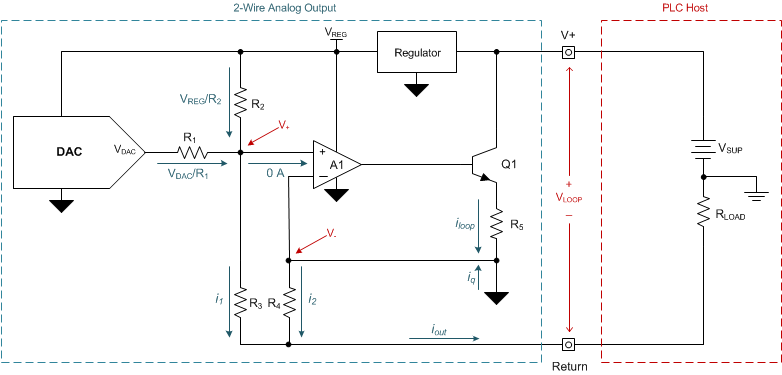
Figure 2: Analysis of typical 2-wire transmitter
Amplifier A1’s chief purpose in “life” is to do whatever it has to on the output to ensure that the inverting and non-inverting input terminals are equal. With this in mind we can assume that under normal operating conditions V+ and V- will be equal. And since V- is connected to loop ground, the V+ potential will also be ground.
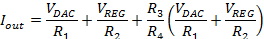
Since V+ is loop ground, or 0V, we can easily define the currents flowing through R1 and R2 as shown in Figure 2. Assuming A1 is an ideal amplifier, the entirety of these currents sum and form i1, which is defined in the equation below.
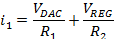
A1 will drive BJT Q1 such that some current flows through R4 along with the return current of all of the components in the design to create the current labeled i2 in Figure 2. Keep in mind that in order to comply with the common 4-20mA communication standard, the current consumption of all components in the design must be <4mA.
Given that the low sides of resistors R3 and R4 are connected to the same node and the high side of each resistor is connected to the input terminals of A1 (which must be at the same voltage potential), we can infer that the voltage drops across R3 and R4 must be equal. We can use this to calculate the value of i2, as shown:


So we can easily see that i2 is simply i1 gained up by the ratio of R3 to R4. This current gain is useful because it allows favorable high impedance loading conditions of the DAC and regulator output, as well as most of the output current to be sourced from the loop directly, rather than from the transmitter itself.
i1 and i2 will sum to form the output current, or Iout. The equations below show this summation and simplify the result to deliver the system transfer function.


The DAC should be selected based on DC accuracy, which is expressed by the static specifications in the datasheet, and minimal current consumption. Some strong candidate DACs for 2-wire transmitter designs are:
Amplifier selection should primarily be based on low input offset voltage and low input bias current since both parameters can skew the ideal transfer function. As with the DAC selection, the amplifier should consume minimal current. Here are a few good choices:
In my follow-up post next month, we’ll look at designing protection solutions for 2-wire transmitters.
Additional resources:
For more information on component selection, PCB layout and measured results on an example discrete 2-wire transmitter design, check out TIPD158. You can also see the industry’s first complete DAC macro models in action.
If you stumbled upon this post while debugging a 2-wire transmitter, I encourage you to check out this series by my colleague, Collin Wells, about common pitfalls in these designs.

