In a previous blog on supply bypassing, I cautioned that poor bypassing could increase distortion of an amplifier. A reader, Walter, asked an interesting question… where should you connect the ground of a bypass capacitor to avoid problems?

This raises questions regarding proper grounding techniques. Wow. Big topic, but I may be able provide some insight with a couple of simple examples.

Figure 1 shows inverting and non-inverting amplifier stages with unintended, parasitic resistance or inductance in the ground connections (highlighted in red). The nodes A, B and C are all intended to be ground. But if current flows in parasitic ground impedances, these nodes will not be at the same potential. It is these parasitic ground impedances that can allow distorted ground currents to contaminate signals.

Walter’s specific question was, “where should you connect the bypass capacitor [the ground side].” It’s an important point. The currents flowing in op amp supply terminals (and therefore the bypass capacitors) may be distorted because they represent only half a sine wave. If distorted (or other interfering) current flows into a vulnerable ground node it can increase the distortion (or other errors) of the amplifier.

An interfering or distorted current flowing into node_A directly affects the ground reference of the input signal, summing in an error. Likewise, a ground current injected into node_B serves as a direct input to the amplifier stage (inverted, in the first circuit). Ground current flowing into node_C directly sums an error with the output voltage. This node may be less vulnerable because the error signal is not amplified by the circuit gain.

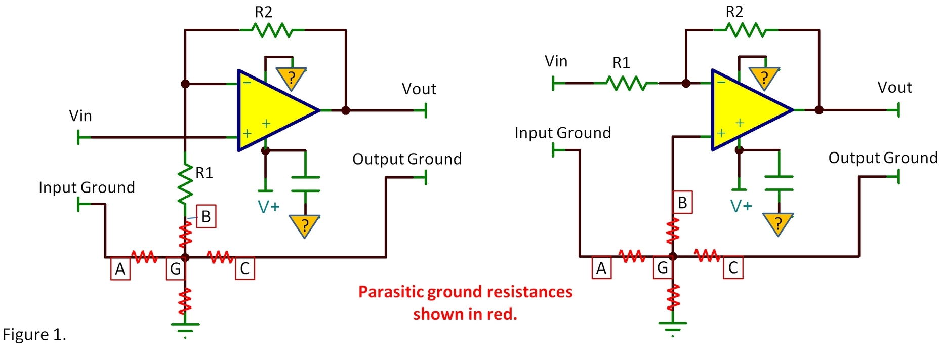
The bypass capacitor should be connected to node_G. Though there may be additional parasitic impedance on its way to other ground points, variation in voltage at node_G affects the critical nodes equally, so it does not inject an error or distortion. I’ve shown an op amp with a single power supply. The ground connection of the op amp (shown on top of the op amp) should also connect to Node_G. A dual (±) supply op amp circuit would have another bypass capacitor for the negative supply and it, too, should connect to node_G.

A solution is to create a circuit board that establishes a ground with the characteristics of node_G. The principle is simple—the circuit trace from the input ground terminal to the ground side of R1 should be a clear path with no connections to contaminating sources of current along the way (figure 2). This input ground trace can join a larger ground connection or ground plane where they meet. With some gain in this stage, output errors are less critical, but you still may want a separate trace to the output terminal connections.

The input ground connection should not connect to equipment chassis at an input connector. This would create an opportunity for other interfering ground noise (such as AC mains ground currents) from impressing current on the clean input ground trace.

A single blog cannot begin to cover all the issues relating to the art of grounding. Woops… did I call this an “art?” It’s science, not art! While, at times, may seem like black magic, Ohm’s law is always at work. Considering where ground currents flow and how they could affect the circuit is always a good start!

Thanks for reading. Comments welcome below,

Bruce

       60 other interesting The Signal topics.

Anonymous
  • Hi Bruce,

    thanks for bringing this topic up.

    Personally, I always recommend to other people (mainly in the Microcontroller world) to separate digital from analog ground, but also current-carrying analog from reference analog ground.

    Even if you have a ground plane, keeping the reference ground separate and free from any significant currents will usually improve signal quality. It is an astonishing and not-so-commonly known fact that even on a ground plane, currents flow not equally distributed. They prefer current paths where a current already flows in opposite direction on another plane/wire above or beneath, causing not evenly distributed voltage potentials on the ground plane and even increased crosstalk. Ths is one of the reasons why a ground plane below a crystal should be isolated form the common ground plane (except for one connection point, of course)

    unfortunately, most layout programs only know one ground and joind it where there is the next possibility. Even when doing a manual layout, it is often difficult to trick the program in keeping the traces separate. SO I usually define three different signals (GND, AGND, RGND) and manually connect them near the supply GND reference point by using a special 'connecting device', mainly a tiny piece of manual copper.

    You're right, grounding is science, but implementing the scientificly calculated grounding paths is an art of its own.

  • Hello Bruce,

    Thank you highlighting another aspect of good grounding. Beside all abstract views additonal two topics impact grounding of bypass capacitors: thermals and vias.

    - Thermals on capacitor's grounding pad act like a resistor and inductor. They are needed to ensure good soldering. Routing wires close by may reduce the number of thermals easily from 4 to 3 to 2 to 1 and result in increase resistance and inductance the other way.

    - Vias: Two vias of 12mil are better than one via of 24mil. Best is arranging 3 small vias around capacitors grounding pad close to thermals (below, left and right) as there is normaly  no space for a 4th via inbetween capacitor's pads.

    Good grounding is not easy, not at all.

    Guenther

  • Thanks Bruce for elaborating.

    I think now I understood what you were saying.

    I read a few articles and found them really informative and interesting!

    Thanks for posting..

  • Anish--  1) Yes, my discussion was primarily focused on the analog portion of a system or an analog-only system. You could infer, however, that a digital ground connecting at points A, B or C could be a very bad situation.

    2) These analog grounds (A, B, C) should come together at a single point. They must necessarily come from some other location to perform their appointed task. As they lead into this common joining point, they should not be tapped along the way with other sources of noisy or distorted ground current. They should make a solo journey to the joining point.

    3) Ferrite beads are used to add a small series inductance, allowing DC current to flow freely while offering a series impedance at high frequency. They might be used a variety of ways to control noise or provide "decoupling" between two portions of a circuit at high frequency. One possible use might be in the joining of a digital and analog ground.

    Hope that helps-- Bruce.

  • Hello Bruce,

    Thanks for sharing this grounding concept. To an amateur like me, it does seems like black magic.

    1. Firstly I would like to ask-This is all going on inside the analog section of the PCB, right?

    2.Do you mean to say that the signal(i/p and o/p) ground should be connected by a single point to

       the analog supply ground? Or you mean to say that the trace connecting this point to supply ground should be

       physically away from this point?

    3. Where exactly should the ferrite beads be used? Only to separate analog and digital grounds?