This thread has been locked.

If you have a related question, please click the "Ask a related question" button in the top right corner. The newly created question will be automatically linked to this question.

A problem about TAS5630 with PBTL mode

Other Parts Discussed in Thread: TAS5630

Hi,

Is there anybody here who can get me out of the trouble brought by TAS5630(Package DKD)?

The Amp board works as the configuration of PBTL BD mode.I'll describe the detailed problem as follows:

It has been powered by a 50V switching power supply which can output 600W power.

        I use another alternative Single-Ended to Differential chip with the gain setting 1.

        I've tested the Amp board by adjusting the amplitude of the 1KHz sin wave input signal.

At the same time,I just monitored the output wave with the oscilliscope on the condition of no load.

        Once the value reached as much as 2V RMS or more than 2V , the output sin wave disappeared correspondingly.

At the same time, the output  wave almost keeped unclipping. 

        It was strange that SD and OTW pins stayed 3.2V all the time after power up.

        Besides that, the OSC pin stopped outputting wave and the output voltage only fell as low as 0.44V .

        The phenomenon seems to result from chip protection itself. During the further debugging, the voltage from VDD keeped as 12V, the temp on the heat slug

        never reached more than 40 centigrades,both of the over current and over load protection can be exclueded since no load condition.

        Now I am wondering the Clipping protection but I've not found the reasonable explanation.

Hope that the problem can be solved ASAP.

        Thanks for your time.  


  • James, I will look into this.  I would like to ask a few questions to help investigate.

    - From what you said above, I think this is your own circuit and layout.  Is that correct?

    - You mention heatslug temperature - are you using a heatsink?

    - If you are not, this could be the problem.  TAS5630 always needs to have its heatsink in place and carefully grounded.  This allows substrate currents to flow directly to ground.  Without this the chip can become confused.  Then I suggest adding a good heatsink and grounding it carefully to the ground plane near the chip.

        (This is specified on page 25 of data sheet SLES220B for TAS5630.)

    - If grounding the heatsink does not improve the situation, we will need to do the following things.  (If it does they may not be necessary.)

    - I will need your schematic and PCB layout in PDF, as well as data sheets for the inductors and capacitors in your LC filters and the decoupling capacitors.

    - If you can, please also let me know what the alternative Single-Ended to Differential chip is.

    - I believe you are saying that SD and OTW pin voltages and heatslug temperature were normal, and you say OSC signal stopped with output signal more than 2Vrms.  But I am not sure about output voltage - does it reach 2Vrms and then stop? or does it continue with clipping?

    Regards,

    Steve.

  • 7144.TAS5630_PBTLMode_BottomRouting.pdf

    Hi,Steve.

    Thanks for your suggestion and clue in time.

      The circuit and PCB layout is made by myself according to the recommendation from TAS5630's datasheet.

           I negelected that the heatsink must be grounded. By contrary, I made keepout nearby the screw mounting area.

    And this can be recognized clearly from the gerber file attached.

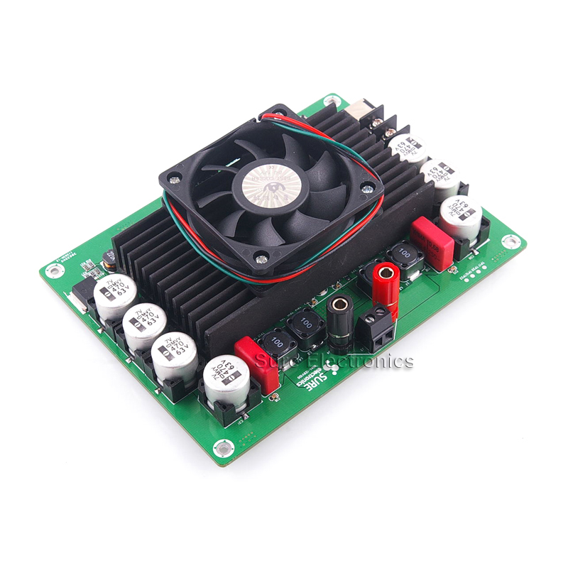
    We've made a aluminum anodizing heatsink with a fan.I'll attched the sample photo.

    Unfounatelly,the surface is not conductive electrically.

           So I tried the equivalent method.

    I also add a copper sheet between the heatsink and the heat slug to enhance the heatsinking capability.

    I just connected a wire between the GND and copper sheet.

    Situation seemed to be a little better now.

    The output wave can reach clipping state with no load when powered by 25V DC.

    At this circumstance, the input sine wave is as high as 3V RMS and the output wave is 11V RMS on one end.

    But the problem emerged once powered by 50V DC.

           The output wave disappears when input signal is more than 2V RMS as I mentioned above.

    And the clipping wave never came out.

    Besides that,I found an odd phenomenon that there seems an 80KHz wave over the peak of 1KHz wave partially.

    It helps upraise the amplitude of output wave.

    I'll attached screen shot of oscillsope later.


    Until now I have not tried with a load and I just prepare for the output voltage which meets the needs at first,

           especially clipping. 

           I attached the PCB layout and schematics.

    And I'm looking forward for your help.

    Thanks again.


  • James, heatsink grounding must be very strong to be effective.  If you used only a single wire to ground the copper sheet, its inductance may be large enough to interfere with good grounding.  I suggest using a wide braid or a broad strip of the same copper and soldering to the copper sheet and to the ground plane with wide solder joints.  Please let me know if this improves your result.

    Also, there may be a problem with your inductors.  Your schematic says they are 10uH/5A.  With only 5A current rating they may be saturating very early.

    Can you try replacing them temporarily with inductors from an EVM?  Please let me know what effect that has.

    Also, can you send me the data sheet for them?

    The 80kHz signal riding on the output is LC filter output ripple, from the switching waveform, because LC filter attenuation is limited at the switching frequency.

    Best regards,

    Steve.