This thread has been locked.

If you have a related question, please click the "Ask a related question" button in the top right corner. The newly created question will be automatically linked to this question.

TPIC8101 Output Signal

Other Parts Discussed in Thread: TPIC8101, MSP430G2553, TMS320F2812

Hello,

My name is Innocentio A. Loe, a newcomer to the forum.

I'm a student at Maranatha Christian University in Indonesia.

Currently, I'm working on a project which is using TPIC8101 as an engine knock detector.

I'm using MSP430G2553 for the microprocessor. The SPI transmission works just fine (I checked the SIMO and SCLK signals using oscilloscope).

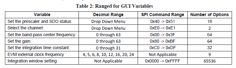
I've tried to use the settings provided in the TPIC8101_Training PDF (7,3 kHz resonant frequency). I only change the INT/HOLD periods. At first I thought that my system works fine, since the output looks like this :

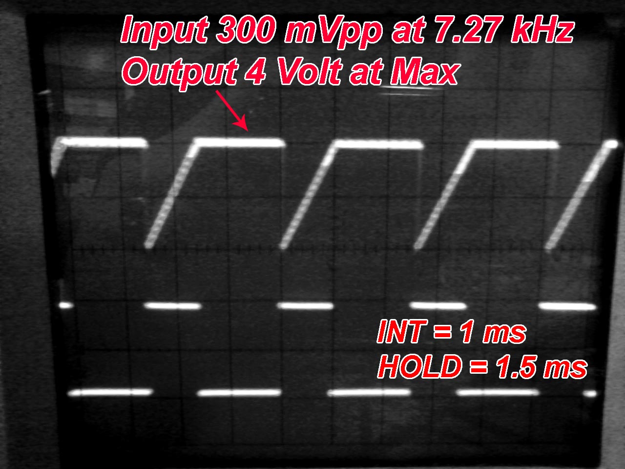
My problem is that the output signal doesn't change on those frequencies or other after I programmed the bandpass filter resonant frequency to e.g. 16 kHz (0x3F) or 1.22 kHz (0x00). I've also checked the output signal using ADC10 module, and found out that the max value (1024) is always at 7.3 kHz frequency, then goes down on lower or higher frequencies.

These are my SPI settings :

    //Data is captured on first SCLK edge, changed on the following edge
    //The inactive state is low
    //SPI Master mode
    //SPI Synchronous mode
    //MSB is transmitted first

These are the codes I've used to program the TPIC8101 :

    set_tpic(); //sets CS and INTHOLD pin low
    spi(0x42); //sets the prescaler - 5 MHz clock, SDO active
    reset_tpic(); //sets CS and INTHOLD pin high
    delay_ms(50);

    set_tpic();
    spi(0xE0); //selects channel 1 as input
    reset_tpic();
    delay_ms(100);

    set_tpic();
    spi(0x2A); //sets the resonant frequency - 7.27KHz
    reset_tpic();
    delay_ms(100);

    set_tpic();
    spi(0x22); //sets the internal gain - 0.381
    reset_tpic();
    delay_ms(100);

    set_tpic();
    spi(0xCA); //sets the integration time - 100 uS
    reset_tpic();
    delay_ms(100);

    while(1)
    {
        int_hold(1000,1500);      //A function that that switches INT/HOLD pin states for a microsecond-based period

    }

I would very much appreciate any help on this subject.

Best regards,

Innocentio A. Loe

MCU

  • Innocentio,

    Welcome to the forum! I think I see your mistake. In your code you write 0x22 to you gain (where the only valid range for gain settings is 0x80 through 0xBF). The band pass frequency setting uses all values from 0x00 to 0x3F.

    It looks like what you are doing is setting the resonant frequency with the first command below and by mistake setting the resonant frequency again with the next set of commands.

        set_tpic();
        spi(0x2A); //sets the resonant frequency - 7.27KHz
        reset_tpic();
        delay_ms(100);

    And then resetting it to:


        set_tpic();
        spi(0x22); //sets the internal gain - 0.381  // This actually sets the band pass again to 5.29 kHz
        reset_tpic();
        delay_ms(100);

    So when you change the top section you dont see a difference since it is immediatly changed to 0x22. Please take a look at the table below that shows the ranges of each setting in the device.

    I beleive to set the gain to 0.381 you should be writing 0xA2. Let me know if that does not work.

    Thanks,

    John


  • Thanks for the reply!

    I've seen now that that error comes because I read the TPIC Training file inaccurately. On page 26 it shows that the internal gain code is 34 in decimal, and 22h in hexadecimal, but I fail to see the binary SPI code beside it, which clearly ads 22h with 80h.

    I've tested it again using the right settings and know it's working properly. Thank you for solving this problem. I got to learn to read datasheets more carefully next time :)


    A question regarding the SPI mode : What is the lowest possible value of SPI clock that I can use? The datasheet only provides 5 MHz maximum SCLK clock-rate, but I prefer to use a slower clock speed to avoid noise.

    Regarding your question about the knock sensor type, I don't know yet which brand I would use, since the project leader haven't decided yet. All I know is that we will use a resonant type knock sensor.

    Best Regards,

    Innocentio A. Loe

  • Innocentio,

    I do not know of a lower limit for the SPI clock rate. It is basically a shift register that just requires the correct amount of clocks during each NCS low period. I think you would be fine with anything in the order of 10kHz to 5MHz. I have sent the question to design to get additional feedback from their perspective.

    Here is a description of the SPI Interface:

    An 8-bit Serial Peripheral Interface (SPI) is integrated into TPIC8101 to communicate with the microcontroller and set various operating parameters. When NCS is high, any signals at CLK and SDI pins are ignored, and SDO is forced into a high impedance state. The input CLK must be low when the signal NCS goes low. At each falling edge of the clock pulse after NCS went low, the new byte is serially shifted into TPIC8101. The byte is shifted with the Most Significant Bit (MSB) first. Only a number of 8 bits per SPI frame is accepted. If a different number than 8 bits is detected, the SPI frame is ignored and the old setting is kept. After the 8th clock pulse, at the next NCS low to high transition, the bits of the SPI shift register are transferred into a latch which allows programming the parameters.

    Also if you don't mind following up once the knock sensor has been chosen for your project, I'd really appreciate it. I want to start keeping track of sensors that customers have used and if there are any problems or issues, so that I can make recommendations moving forward.

    I will follow up when I have heard back from design.

    Thanks,

    John

  • Mr. Griffith,

    Thank you, I will be waiting for your follow up.

    I'll certainly send you the information about the knock sensor brand and code, but I guess it would take some time for the project leader to decide, maybe around the end of November. Having the TPIC worked the right way now, we will start working on finding its output characteristic first using function generator input, so we can determine the most suitable knock sensor for our engine later.

    Thanks,

    Innocentio

  • Innocentio,

    I just heard back from one of the designers, and they verified that there is not usually a lower limit on SPI as long as all you are following all of the edge timing requirments on page 7 of the datasheet. No simulations were run but you should be just fine running a much slower SPI clock rate. Let me know if you run into any issues.

    John

  • Thanks for the info Sir.

    I've tested it at lab using 1 kHz SCLK. So far, I haven't found any problems.

    For your info : We've decided the knock sensor type, which is Hyundai 39250-22010, something like this : http://www.autopartoo.com/oem/hyundai/3925022010.html

    I'll inform you later if we find issues while using this sensor. Thanks again!

    Inno

  • Thanks Innocentio for following up! I appreciate it.

    John

  • Hi,I am facing issue while getting out from TPIC8101.I programmed TPIC with required parameters as per data sheet.But the output pin was going high regardless of if the sensor was connected or if it was open circuited.
    Please help me if you have experience about this issue.it is very urgent to me.Please help

  • Hi there,

    I've encountered this issue before, and found that the problem is that my SPI settings isn't right. But first please check these following pins :

    1. Do you have the CS pin controlled? It should be pulled low at the start of a transmission and pulled high at the end of it.

    2. Is TEST pin pulled high? You should pull it high or left it unconnected to be able to program the chip.

    3. Do you pull-down the INT pin at each transmission start and pull it high again later?

    A schematic will be helpful, and you could post your SPI initialization code and list of commands which you've sent to the TPIC.

    A good way to check the problem is to receive the echo from SDO pin. Every time you send a command to TPIC via SDI pin (in normal mode), the SDO pin will echo the same command at the next transmission.

    Regards.

  • Hi Innocentio,

    Thanks for reply.

    1)spi intilialization part is

      /*Set the character length to 8 bits and SPI SW reset bit to 1 in
            the SPI configuration control register*/
     

    SPI_BAUD is 5Mhz

        Clock setting is raising edge without delay mode


    1)all spi messages are in one array as shown below


    Spi_msg_array[TPIC_TX_PRESCALER] =    0x0046;8Mhz prescalar
    Spi_msg_array [TPIC_TX_CHANNEL] = 0x00E0;//channel 1 on tpic ic      Spi_msg_array [TPIC_TX_BAND_PASS] =    0x003A;//00 D[5:0](15.07khz)
    Spi_msg_array [TPIC_TX_GAIN] =   0x00B2;//(10 D[5:0])//0.191 decimal 50
    Spi_msg_array [TPIC_TX_INT_TIME_CONST] =0x00D8;//(110 D[4:0]) //320us Spi_msg_array [TPIC_TX_SPI_CONFIG] = 0x0071; /* Set advanced SPI mode */


    2) these messages are transmitted using below code


    for(det_spi_byte_index =0;det_spi_byte_index < sizeof(Spi_msg_array);det_spi_byte_index++ )
       {
       /*set chip select low*/
        chip_select(CHIP_SEL_LOW);

       /*INT/HOLD pin is making low by writing zero in corresponding PWM PIN*/

    GpioDataRegs.GPADAT.bit.GPIOA5 =0;
         

       /*update the TX buff with command*/
       SpiaRegs.SPITXBUF =((det_spi_tx[det_spi_byte_index]));


       /*wait until the byte is shifted out*/
       while ( SpiaRegs.SPISTS.bit.INT_FLAG != 1) ;

       /*update the TX buff with command*/
     
       /*Read RX buffer*/
      det_spi_rx[det_spi_byte_index] = SpiaRegs.SPIRXBUF>>8;
     
      SpiaRegs.SPITXBUF =((det_spi_tx[det_spi_byte_index])>>8);


       /*wait until the byte is shifted out*/
       while ( SpiaRegs.SPISTS.bit.INT_FLAG != 1) ;

    SpiaRegs.SPIRXBUF;  
       /*set chip select high*/
       chip_select(CHIP_SEL_HIGH);
       /*INT/HOLD pin is making high by writing zero in corresponding PWM PIN*/


    GpioDataRegs.GPADAT.bit.GPIOA5 =1;
      
       Delay(10);
      
      
       }

    3)I am comparing  det_spi_rx[] with det_spi_tx[] to validate transmission.id it write thing to chevk data on rx_buf after transmitting or not.Plesae let me know.


    4)Test pin is left unconnected


  • Hi Sandhya,

    The bits are shifted in on the falling edge of the clock not the rising edge. You wrote the following:

    SPI_BAUD is 5Mhz

        Clock setting is raising edge without delay mode

    I think you need to change this to falling.

    Thanks,

    John

  • Jhon,

    spi is initilized with clock freq as 1Mhz,falling edge without delay mode.in my project,f2812 single CS signal is selecting for 3 devices using Multiplexer selection lines.

    The input for TPIC is a 15Khz squre wave

    after spi communication  a 4ms squre wave is generating to read TPIC.i am always reading max voltages.

    In my project,the hw which i am using is not having controller and this TPIC ic back end.It is very difficult to check the values at pins

    I am trying to read OUT value through ADC pins of controller.Please help me where could be the mistake in my code.


  • Hello again there, Mr. Griffith

    To Sandhya :

    As stated above, your SPI clock polarity setting is wrong. It should be falling edge instead of rising edge.

    Also I'm curious about your PWM. At your program I only found that you pull the INT/HOLD pin low at the start of transmission, and pull it high again after it. But did you turn it On-Off continuosly?

    I only saw that you turn it on again at the end of transmission but I see nothing which toggles it continuosly. (Since you are using GPIO pin, I assume that you use delay function, but CMIIW).

    In my case, I use a timer interrupt to create PWM for INT/HOLD pin.

  • John,Thanks for quick response.

    1)clock setting i have modified from rasing edge to falling edge.but it is not working

    2)Regarding INT/HOLD signal

    At intilization i made PWM INPUT PIN which is acting as INT/HOLD for TPIC  to output pins  and written zero in it.

    During SPI tranmission i have written ZERO in it to make the pin low.

    after spi tranmission completes I am enabling Timer enable bits to generate a PWM wave with 2ms ON AND 2MS off PERIOD BY SETTONG counter and period registers.

    interrupt will be invoked for every 2ms in this routne i am making this pwm pin 0 and 1 (to high period and low period) by EXCLUSIVE ORING THE BIT.

  • Well, since don't post any hardware image I can't check if your hardware setting is correct or not.

    But I found one miss in your code. Did you return RESET bit of the SPI to 0 after initialization? Because I didn't find that you did it (unless you just didn't wrote it in your post). If you kept the RESET bit to 1 after initialization, your MCU won't do any SPI transmission.

    Also what kind of MCU you are using? If it is MSP430 type, I can share my code on TPIC and SPI initialization (which have worked). I'm using MSP430G2553.

  • Hi Sandhya,

    The other thing that caught my eye when going through your code is you set the clock prescaler to 8MHz, and then you said two messages ago the following:

    spi is initilized with clock freq as 1Mhz,falling edge without delay mode.in my project,f2812 single CS signal is selecting for 3 devices using Multiplexer selection lines.

    Looks like Innocentio had some feedback as well. Thanks Innocentio!

    John

  • John,

    I have configured SPIBRR equal to Mhz while SPI initilizations.The max value of spi clock is 5Mhz as per f2812 spi data sheet.

    I have send 8Mhz prescalar to program TPIC8101 through SPI using "0x46",As per my prject requirement

    These two values should be same?please let me know.

  • Innocentio,

    I am using tms320F2812 ascontroller  in my project.

  • No.

    The SPI clock doesn't need to be the same with the XIN-XOUT clock.
    You see, the prescaler is used to rescale XIN-XOUT clock to the actual internal ADC clock of the TPIC8101.

    Now, how do you give clock to the XIN-XOUT pin? Using a crystal resonator? If yes, did you put a bias resistor as per datasheet requirement? If you control XIN-XOUT clock using your microcontroller, then you should use the schema available at the datasheet, with precise clock controlling (using timer interrupt perhaps)

    Since you are using a different type microcontroler, I don't think that my program could help you that much, except if you want to study it.

  • Hi,

    I think I am failing at spi communication

    spi initilaizations are:

     Reset on, clk pol=1 : Falling edge, 8-bit char bits

    Enable master mode

    Baud rate as 1 MHz

    Relinquish SPI from Reset.

    spi transmission is like beolw:

    int_hold(low)

    //chip select low
    chip_select(0);

    SpiaRegs
    .SPITXBUF =0x0046;
    while ( SpiaRegs.SPISTS.bit.INT_FLAG != 1) ;
    SpiaRegs
    .SPIRXBUF;

    SpiaRegs
    .SPITXBUF =(0x0046)<<8;
    while ( SpiaRegs.SPISTS.bit.INT_FLAG != 1) ;
    SpiaRegs
    .SPIRXBUF;
    chip_select(
    1);

    chip_select(
    0);

    SpiaRegs
    .SPITXBUF =0xE000;
    while ( SpiaRegs.SPISTS.bit.INT_FLAG != 1) ;
    SpiaRegs
    .SPIRXBUF;

    SpiaRegs
    .SPITXBUF =(0xE000)<<8;
    while ( SpiaRegs.SPISTS.bit.INT_FLAG != 1) ;
    SpiaRegs
    .SPIRXBUF;

    chip_select(
    1);

    chip_select(
    0);

    SpiaRegs
    .SPITXBUF =0x3A00;
    while ( SpiaRegs.SPISTS.bit.INT_FLAG != 1) ;
    SpiaRegs
    .SPIRXBUF;

    SpiaRegs
    .SPITXBUF =(0x3A00)<<8;
    while ( SpiaRegs.SPISTS.bit.INT_FLAG != 1) ;
    SpiaRegs
    .SPIRXBUF;
    chip_select(
    1);
    chip_select(
    0);

    SpiaRegs
    .SPITXBUF =0xB200;
    while ( SpiaRegs.SPISTS.bit.INT_FLAG != 1) ;
    SpiaRegs
    .SPIRXBUF;

    SpiaRegs
    .SPITXBUF =(0xB200)<<8;
    while ( SpiaRegs.SPISTS.bit.INT_FLAG != 1) ;
    SpiaRegs
    .SPIRXBUF;
    chip_select(
    1);

    chip_select(
    0);

    SpiaRegs
    .SPITXBUF =0xD800;
    while ( SpiaRegs.SPISTS.bit.INT_FLAG != 1) ;
    SpiaRegs
    .SPIRXBUF;
    SpiaRegs
    .SPITXBUF =(0xD800)<<8;
    while ( SpiaRegs.SPISTS.bit.INT_FLAG != 1) ;
    SpiaRegs
    .SPIRXBUF;
    chip_select(
    1);

    chip_select(
    0);

    SpiaRegs
    .SPITXBUF =0x7100;//(Lsh 0x71)
    while ( SpiaRegs.SPISTS.bit.INT_FLAG != 1) ;
    SpiaRegs
    .SPIRXBUF;

    SpiaRegs
    .SPITXBUF =(0x7100)<<8;//(Lsh 0x71)
    while ( SpiaRegs.SPISTS.bit.INT_FLAG != 1) ;
    SpiaRegs
    .SPIRXBUF;

    chip_select(
    1);

    int_hold(low)

    INT/HOLD pin is from controller.int/hold pin is low at the time of spi transmission and high later using timer  interrupt.This is working checked at that pin.

    i checked OUT pin of TPIC,it is comming to high state only  in 400us and hold in it for remaining 3.6ms.but as per data sheet it should reach to high with total ON period and hold for off period.

    Please help me where could be the issue.


  • Well, I don't know mandatory or not, but the way I do thing is like this :

    1. Pull CS and INTHOLD pin LOW

    2. Send the SPI command

    3. Pull CS and INTHOLD back HIGH

    The way I see you do things is that you only pull CS pin back high at each command but left the INTHOLD pin Low. Also at the end of the transmission you write it low again. Why?

    Also, for the way you send your command :

    SpiaRegs.SPITXBUF =0xD800;
    while ( SpiaRegs.SPISTS.bit.INT_FLAG != 1) ;
    SpiaRegs
    .SPIRXBUF;
    SpiaRegs
    .SPITXBUF =(0xD800)<<8;
    while ( SpiaRegs.SPISTS.bit.INT_FLAG != 1) ;
    SpiaRegs
    .SPIRXBUF;
    chip_select(
    1);


    Nah, you sent the command 0xD8, but since the TX Buff is only 8 bits, it will translate to 0x00. Also you sent it again with LSB shifted. IMHO it will cause the TPIC to read the command as Band-Pass Center Frequency (See table in datasheet). All other commands will be neglected. Check that out

    And no, the output doesn't exactly need to reach HIGH at the end of ON period, but rather reaching the last integration value.

  • Innocentio,

    Thanks for reply,

    1)made int/hold high and low before and after each message

    2)My controller, TXBUFF AND RX BUFFER size is 16 bits,and transmit bufer is left justified,because of that reason i sent messages as explained above,but i understood ur point and modeified the software by sending only one time by leftshifting,that is

    SpiaRegs.SPITXBUF =(0xD800)<<8;
    while ( SpiaRegs.SPISTS.bit.INT_FLAG != 1) ;
    SpiaRegs
    .SPIRXBUF;

     3)I observe the OUT voltage always 4.8v whether sensor connected or left it as open


  • Well... Since it seems that your code has no problem, I would think that the fault is at the IC or perhaps the clock source. Since you haven't care to post any schematics then I couldn't help any further

  • Innocentio,

    Well I am ablr to check signals at hardware by opening my ECU,I will send you more details on code and schematica.Please can you share your email_id.

  • Sorry for the wait.

    Well, why not just attach those stuff here?

    Also I've noticed that you have checked this other thread :

    http://e2e.ti.com/support/microcontrollers/c2000/f/171/t/49355.aspx?pi269061=2

    If you're able to, I suggest you to check the SPI SIMO and SOMI pins using oscilloscope like others did to be sure that your data is transmitted.

    I've had an issue with MSP430 clock source before, that I have to calibrate it manually while checking the Clock Output pin. This problem with clock source causes every SPI transmission to fail. I have to calibrate the clock register to find the best result possible.

    I don't know about your clock source, but you can check on my other thread here regarding my internal clock problem : http://e2e.ti.com/support/microcontrollers/msp430/f/166/p/239057/841977.aspx

    I have no experience with F2812 so I can't say whether your SPI initialization code has minor flaws or not (that would require some learning on the datasheet :( ).

  • Oh, and one more thing :

    If everything up till now fails, maybe you can use bit banging method for the SPI transmission as I did before with TPIC8101 and ADXL sensors.

    Bit banging always works for me, as long I follow the SPI interface timing diagram right.