This thread has been locked.

If you have a related question, please click the "Ask a related question" button in the top right corner. The newly created question will be automatically linked to this question.

DDR LVDS interface between ADS5560 and XILINX SPARTAN-6 150 FPGA

Other Parts Discussed in Thread: ADS5560, CDCE72010

hi,

In the current project, we use ADS5560 whos sampling rate is 30.72MHz, and the sampled data is transferred to Spartan6 through DDR LVDS parallel port.

the sample clock signal into ADS5560 is generated by CDCE72010, and AC coupled through a transformer. The differential clock after the transformer and before

ADS5560 is shown as follows,


The DDR data line pair is shown as follows


but the clock signal of ADS5560 output is distorted very severely, whos duty cycle is far from 50%.  the pcb board ground plane is spilt into AGND and DGND sub-plane. ADS5560 is mounted on AGND, and Spartan on DGND.  Ground plane may cause impedance discontinuity, but the degree of effect is unkonw now, and the data line pair seem to work well, since that the problem clock line pair may have no relation to the split. what is the possible cause?

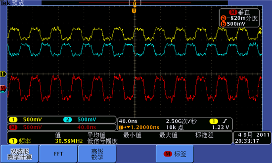
  • the sample rate in the current project is 30.72Mhz, and change ADS5560 into high mode, it works well. the clockout from ADC to FPGA is shown as below. the red trace is clockout_p minus clockout_m.

  • Hi, 

    After looking over the plots, the non-50% duty cycle of the CLKOUT is normal since the operating condition of the ADS5560 is at 30.72MHz with Low Speed Mode enabled. 

    It is often easier to meet setup/hold time at lower clock rate than at higher clock rate. At low speed mode, the internal delay lock loop (DLL) is disabled, and this DLL circuit is used at high speed mode to correct the CLKOUT's duty cycle for optimal setup/hold time of the data.

    Even with non-50% duty cycle, we still have a minimum setup/hold time on page 8 of the ADS5560 datasheet. The minimum setup/hold time is listed as 2ns and 2ns, respectively. This may be used as guaranteed setup/hold time for the FPGA when using CLKOUT as reference. You can refer to attached diagram to see how low speed mode does not change the data valid window. 

    For 30.72MHz of sample rate, I recommend keeping the ADS5560 in high speed mode since the limit for low speed mode is 30MHz and below. 

    -KH