This thread has been locked.

If you have a related question, please click the "Ask a related question" button in the top right corner. The newly created question will be automatically linked to this question.

PCM5122 DAC as I2S master troubles with PLL mode

Other Parts Discussed in Thread: PCM5122

I'm working on a new project and I'm trying to use the PCM5122 DAC clocked by a 12 MHz oscillator as I2S master (the DAC generates BCK and LRCK signals). My goal is to achieve what stated at page 22 of PCM5122 datasheet which says:

"SCK rates that are not common to standard audio clocks, between 1MHz and 50MHz, are only supported in software mode by configuring various PLL and clock-divider registers. This programmability allows the device to become a clock master and drive the host serial port with LRCK and BCK, from a non-audio related clock (for example, using 12MHz to generate 44.1kHz (LRCK) and 2.8224MHz (BCK) )."

so I think it should be possible if it's reported as example on the datasheet.
I'm using the DAC as shown on page 17 of the datasheet:

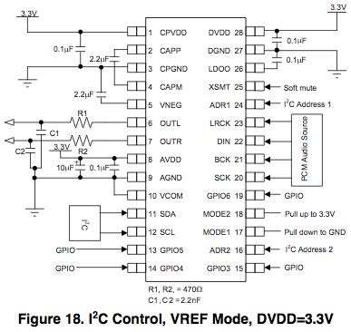
with a 12 MHz oscillator connected to the pin 20 (SCK).
In order to get proper audio clocks from a 12 MHz oscillator we have to use the internal PLL so I put an eye on Figure 26 of the datasheet (page 24)


and found some troubles:

1) How it's possible to generate precise BCK and LRCK from a 12 MHz source if BCK and LRCK outputs are generated from SCK only?
BCK and LRCK dividers should be clocked by the PLL output not directly from SCK. In fact I'm only able to generate LRCK and BCK by dividing the 12 MHz SCK leading to unprecise results. I'm sure I'm missing something.

2) SRCREF register is meant to select the clock input for the PLL between 4 different possibilities. If you look at register 13 description (page 81 on the datasheet) you got simply the bit 4 that le you choose between SCK and BCK as PLL clock input

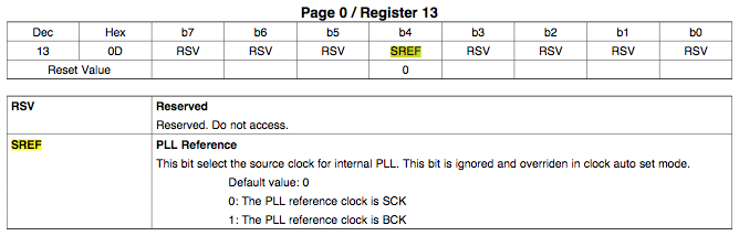
Finally page 23 says:

"The source reference clock for the PLL reference clock is selected by programming the SRCREF value on Page 0, Register 13, D(6:4)."

reporting to use bits 6 to 4 of register 13 to set the PLL input (how?). I'm confused, someone knows wich is the truth?

3) In figure 26 there is a SRCDAC to route clock to DAC, charge pump and digital filter modules. The point here is that SRCDAC register does not exists or is completely missing from the documentation. So, the question is, where the DACCK comes from?

Even with the above problems I did my best to let the PCM5122 acting as I2S master using PLL mode (trying to play at 44100 KHz 16 bit). The registers config I'm using without success are the following:

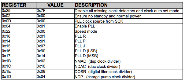
I got 12 MHz output on both LRCK and BCK (leaving their dividers as 0x00) and no CPCK. If I set the BCK and LRCK dividers to values different from 0 I got 990.312 KHz as charge pump clock.
The clock is obviously not correctly routed and the PLL is not clocking the LRCK and BCK signals but I'm not able to see what's wrong (please note that I'm using values from datasheet example to set PLL coefficients P, J and D).

Sorry for the very long post, I hope someone is able to fill the holes in the datasheet as TI support told me to report my problems on the forum!

Thanks in advance

Best Regards

Marco 

  • Marco,

    thank you for going through the datasheet in such fine detail. I understand the issue you're having, and will work with one of the application engineers for the product to respond to you. The PCM512x and 4x datasheets are going through a cleanup in the next few weeks. I hope to have more details on this application very soon. (of course, we'll answer in this thread before the datasheet gets updated!)

    Thanks again

    Dafydd Roche

  • Thank's a lot for you for the prompt feedback, hope to hear you soon!

    Marco

  • Marco,

    datasheets are under revision to clarify this.

    In the hardware domain, you will have to use 2 pins to bring in your 12MHz, into the PLL, then out of a GPIO. 

    That GPIO will then be externally connected to the SCK (master clock in. The device will think that you are in-fact bringing in an audio rate BCK.

    Please let me know which GPIO you would like to bring your 12MHz in on, and which your like your Audio Master Clock output on.

    I will provide the specific register writes to achieve that functionality. (before we get the datasheet cleaned)

    Best regards

    /DAfydd

  • Glad to hear you DAfydd,

    thank you for your clarification. I would like to use a 12 MHz DIGITAL OSCILLATOR which should be connected to a 1 pin only, is it possible or I have to use a crystal connected between 2 GPIO pins? Let me know what is supported and what do you suggest. GPIO4 and GPIO5 in my opinion are good candidates to input the 12 MHz to the chip if 2 pins are required (GPIO3 is better if only one pin is enough using a digital oscillator).

    GPIO 6 is close to the SCK pin, so we can use this pin as PLL output and connect it to SCK pin easily.

    Hope to hear you soon.

    Many Thanks

    Regards

    Marco 

  • Marco,

    Use GPIO3 for your 12MHz CMOS 3V3 input, and GPIO6 for output from the PLL.

    The PCM512x does not have the oscillator circuit to connect the XTAL to.

    I will post later with recommended software register settings.

    /Dafydd

  • Ok, GPIO3 (in) and GPIO6 (out) are good for me

    thanks

    Marco 

  • Any (good) news?

    Thanks

    Marco 

  • The issue is becoming urgent, my project is blocked, I need to know If there will a solution in the near future or if I have to find another DAC.

    Many Thanks

    Marco 

  • Marco,

    I was trying to get the catalog datasheet edits done to include this, but as this is urgent, please try the following things:

    Set Auto Clock Config Off using Page0 / Reg 37 (0x25) with data 0bXXXXXX0X (where X = do not overwrite this)

    Set GPIO3 to input in page 0 / register 8 (0x08)

    Set PLL Reference to GPIO using  Page 0 / Reg 13 (0x0D) with the data 0b0011XXXX (where X = do not overwrite this) 

    Set GPIO Source for PLL Reference CLK to GPIO using Page 0 /Reg 18 (0x08) with the data 0b00000010


    // That should enable the PLL to use GPIO3 as a clock input,

    // You should now configure your PLL as you need based on your incoming clock frequency and desired output.


    // now we need to set GPIO 6 as an output.

    Set GPIO6 as an output using page 0 / register 8 (0x08)

    Set GPIO6 GPIO output source in Page 0 / Reg 85 (0x55) to be 0b00010000 (PLL /4)

    //GPIO 6 should now be putting out a pretty nice master clock that you can route externally to the device and drop into the SCK input.

    // You'll then need to configure your serial port divider ratio's manually.

    I believe this should work for you, but let me know how you get on and we'll have one of our apps engineers delve in further.

    Thanks again

    Dafydd

  • Thank you Dafydd for your help,

    unfortunately I was not able to achieve the desired result, nothing comes out from my GPIO6. I have some dubts, you say to disable Auto clock set by writing a 0 to register 0x25

    Dafydd Roche said:
    Set Auto Clock Config Off using Page0 / Reg 37 (0x25) with data 0bXXXXXX0X (where X = do not overwrite this)

    but the datasheet reports that in order to disable the Auto clock feature I have to write a 1. Could you confirm which way is correct please?
    Another thing which is not clear to me is the register to use for setting the PLL reference clock to GPIO:

    Dafydd Roche said:
    Set GPIO Source for PLL Reference CLK to GPIO using Page 0 /Reg 18 (0x08) with the data 0b00000010


    is it register 18 or 0x08 or another?
    In your opinion, after setting these register values should I expect immediately something out from GPIO6 or do I need at least to enable the PLL (register 4 set to 1)?

    Thanks a lot for your assistance

    Regards

    Marco
     

  • Marco, I finally had some lab time these last few days.

    please try the following script:

    ## Master mode implemented by only 12MHz CLK

    ## Connection

    # GPIO5 : 12MHz CLK input
    # GPIO3 : PLLCLK_OUT (24.576MHz), which must be connected to SCK pin
    # SCK : must be connected to GPIO3 to input 24.576MHz from PLLOUT
    # BCK : output terminal, which must be input to BCK terminal of AP2 through dumping res of 1kohm (Need pull-up resistor)
    # LRCK : output terminal, which must be input to LRCK terminal of AP2 through dumping res of 1kohm (Need pull-up resistor)
    # DATA : input from external data source

    #### Clock Flex Mode ######################
    # page 253
    w 98 00 fd
    # set Flex Register A
    w 98 3f 11
    # set Flex Register B
    w 98 40 ff
    # page 0
    w 98 00 00
    ############################################

    #### CLK divider setting ###################
    # Auto divider setting : disable
    w 98 25 7A
    # PLL P divider
    w 98 14 00
    # PLL J divider
    w 98 15 08
    # PLL D1 divider
    w 98 16 07
    # PLL D2 divider
    w 98 17 80
    # PLL R divider
    w 98 18 00
    # miniDSP CLK divider
    w 98 1B 01
    # DAC CLK divider
    w 98 1C 0F
    # NCP CLK divider
    w 98 1D 03
    # OSC CLK divider
    w 98 1E 07
    # FS setting
    w 98 22 00
    # IDAC1
    w 98 23 04
    # IDAC2
    w 98 24 00
    #############################################

    #### Master mode setting ####################
    # PLL REF from GPIO
    w 98 0D 30
    # GPIO5 => PLL REF
    w 98 12 04
    # BCK, LRCK output
    w 98 09 11
    # Master mode BCK, LRCK divider reset release
    w 98 0C 7F
    # Master mode BCK divider setting
    w 98 20 07
    # Master mode LRCK divider setting
    w 98 21 3F
    # GPIO3/4 OE
    w 98 08 0C
    # PLLCLK/4 => GPIO3
    w 98 52 10
    # PLLLOCK/4 => GPIO4
    w 98 53 0A
    ##############################################

    #### Stand-by request and release ############
    # Stand-by request
    w 98 02 10
    # Stand-by release
    w 98 02 00
    ##############################################

  • Thank you Dafydd for trying this solution,

    I'm pretty sure that each line of your script means something like

    write 98 <value> <register>

    but I was wondering what 98 means. Is that correct? May I ignore the costant 98 value to implement my driver?

    Thanks a lot

    Marco 

  • #Format:
    #Commands are written in the TI script for I2C.
    #A BB CC DD

    #A = R or W (read or write)
    #BB = I2C Address (98 in this case)
    #CC = Register
    #DD = for Writes, it's the data, for reads, it's the number of bytes to read back.

  • Hi Dafydd,

    Finally I got the DAC working thanks to your istructions. There are some details to improve but the system now is working. I hope to view the updated datasheet when I'll be back from my summer holidays!

    Thanks a lot for your precious support Dafydd and enjoy your holidays

    Best Regards

    Marco 

  • Hi,

    are there any news for the updated data sheet? 

    Regards

    Daniel

  • Daniel Matuschek1 said:
    are there any news for the updated data sheet? 

    Same here,the datasheet is still no documenting  like source clock for internal PLL with four input.

    I need to use BCK to generate SCK.

  • Hi Dafydd, are there any news on the updated datasheet?

    Regards

    Rafael