This thread has been locked.

If you have a related question, please click the "Ask a related question" button in the top right corner. The newly created question will be automatically linked to this question.

Need Help! I can't get DAC34h84evm output based on my configuration.

Other Parts Discussed in Thread: FMC-DAC-ADAPTER, CDCE62005, DAC34H84, DAC34SH84, DAC3482

Hi all,

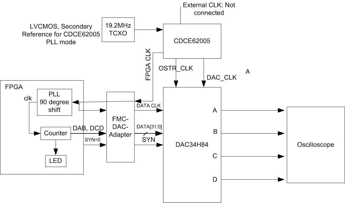
I encountered some problems when testing the dac34h84evm. The DAC board is connected with the Xilinx VC-707 FPGA board using the FMC-DAC-adapter.

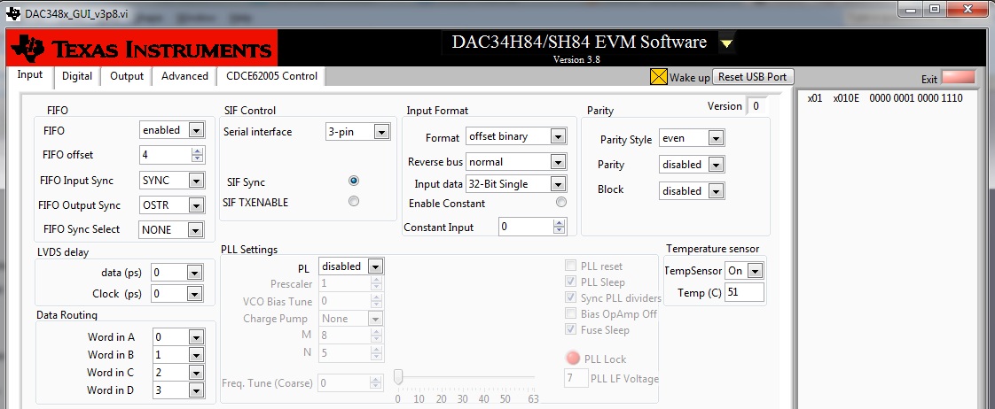
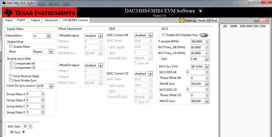
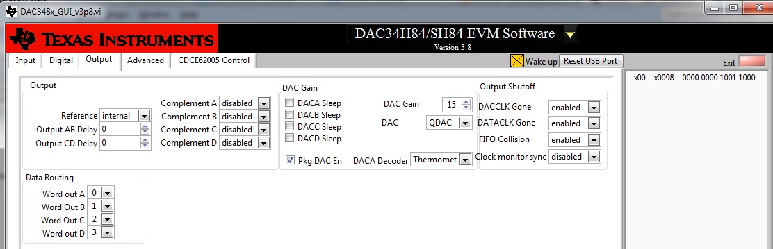
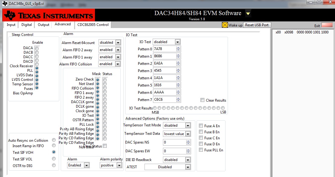
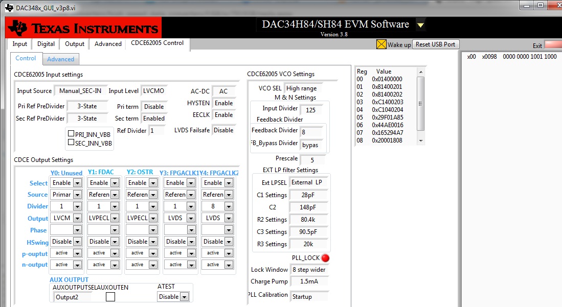
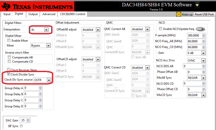
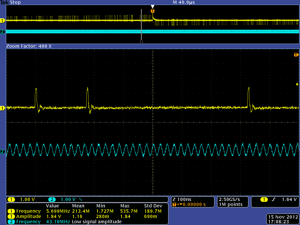
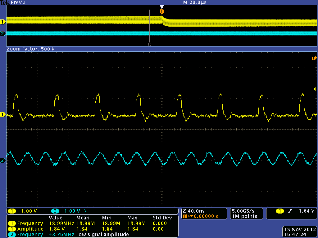
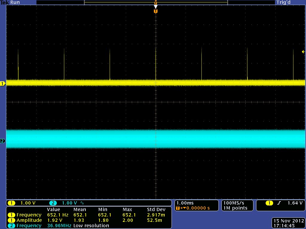
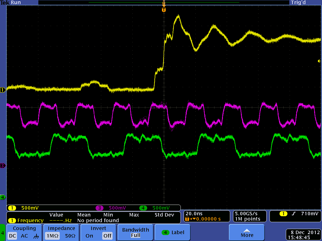
The clock for data (DCLK) is from the CDCE62005 whose frequency is 19.2 MHZ, the same as DAC's input clock (DAC_CLK). Data is center-aligned. We use the software(DAC348x EVM Software GUI (Rev. B) ) to configure it. Only FIFO is enabled and x1 interpolation. But we don't get the analog output on the oscilloscope. Whatever data we input. i.e. DA=DA+1 or constant value, we get nothing but some pulses. 


I checked the connection of FMC on FPGA to FMC-DAC adapter which is correct, so i don't think the input "DA" is wrong. So I don't know exactly what goes wrong. Please help. You can reach me at jamesfade_1234@hotmail.com or this reply. Thanks a lot.


I attach my VHDL interface code. 

--===================================
--             intf_TI_dac34h84evm 
-- Description: This module is used to connect with FPGAs with HSMC port for Terasic ADA
--				(1) data is center-aligned. 
--==================================
library ieee;
use ieee.std_logic_1164.all;
use ieee.std_logic_arith.all;
use ieee.std_logic_unsigned.all;

-- obufds library
Library UNISIM;
use UNISIM.vcomponents.all;

library work;
		
entity intf_TI_dac34h84evm is
port (	
		FPGAOUT_CLKP_I	: in std_logic;
		FPGAOUT_CLKN_I	: in std_logic;
		
		--PARITYP			: out std_logic;						--PARITYABP: Sync the FIFO pointer or act as a parity input for the AB-data bus
		--PARITYN			: out std_logic;
		SYNCP			: out std_logic;						--SYNCP: allow complete reversal of the data interface when setting the rev_interface bit in register config.
		SYNCN			: out std_logic;
		-- FIFO_ISTRP		: out std_logic;						--ISTRP: act with SYNC, PARITY.
		-- FIFO_ISTRN		: out std_logic;
		DATA_CLKP		: out std_logic;						--DATACLKP: LVDS positive input data clock. Data are lutched on both edges of DATACLKP/N.
		DATA_CLKN		: out std_logic;
		
		IO_DAP			: out std_logic_vector (15 downto 0);	--DAB: data for AB-channel
		IO_DAN			: out std_logic_vector (15 downto 0);
		
		IO_DBP			: out std_logic_vector (15 downto 0);	--DCD: data for CD-channel
		IO_DBN			: out std_logic_vector (15 downto 0)
		
	 );
end intf_TI_dac34h84evm;

Architecture Behavior of intf_TI_dac34h84evm is

------------ components ------------
component pll_div is
port(
	clkin : in std_logic;
	rst : in std_logic;
	pwrdwn : in std_logic;
	clkout0: out std_logic;
	clkout1: out std_logic;
	clkout2: out std_logic;
	clkout3: out std_logic;
	clkout4: out std_logic;
	clkout5: out std_logic
	);
end  component pll_div;
------------

signal		clk				:	std_logic;
-- signal		PARITY			:   std_logic;
signal		SYNC			:   std_logic;
-- signal		FIFO_ISTR		:   std_logic;
signal		DATA_CLK		:   std_logic;

signal		IO_DA			:   std_logic_vector (15 downto 0);
signal		IO_DB			:   std_logic_vector (15 downto 0);

signal		clkin			: std_logic;
signal		FPGAOUT_CLK		: std_logic;

begin
--=======================================================
--                  Dac34h84evm outputs
--=======================================================
--PARITY
-- OBUFDS_inst_PARITY : OBUFDS
   -- generic map (
      -- IOSTANDARD => "DEFAULT")
   -- port map (
      -- O => PARITYP,
      -- OB => PARITYN,
      -- I => PARITY
   -- );
--SYNC
OBUFDS_inst_SYNC : OBUFDS
   generic map (
      IOSTANDARD => "DEFAULT")
   port map (
      O => SYNCP,
      OB => SYNCN,
      I => SYNC
   );
--FIFO_ISTR
-- OBUFDS_inst_FIFO_ISTR : OBUFDS
   -- generic map (
      -- IOSTANDARD => "DEFAULT")
   -- port map (
      -- O => FIFO_ISTRP,
      -- OB => FIFO_ISTRN,
      -- I => FIFO_ISTR
   -- );
--DATA_CLK
OBUFDS_inst_DATA_CLK : OBUFDS
   generic map (
      IOSTANDARD => "DEFAULT")
   port map (
      O => DATA_CLKP,
      OB => DATA_CLKN,
      I => DATA_CLK
   );
--IO_DA
IO_DA_GEN: for j in 0 to 15 generate
begin
	OBUFDS_inst_IO_DA : OBUFDS
	   generic map (
		  IOSTANDARD => "DEFAULT")
	   port map (
		  O => IO_DAP(j),
		  OB => IO_DAN(j),
		  I => IO_DA(j)
	   );
end generate IO_DA_GEN;
-- IO_DB
IO_DB_GEN: for j in 0 to 15 generate
begin
	OBUFDS_inst_IO_DB : OBUFDS
	   generic map (
		  IOSTANDARD => "DEFAULT")
	   port map (
		  O => IO_DBP(j),
		  OB => IO_DBN(j),
		  I => IO_DB(j)
	   );
end generate IO_DB_GEN;
IBUFDS_inst_FPGAout_clk : IBUFDS
   generic map (
      DIFF_TERM => FALSE, -- Differential Termination 
      IBUF_LOW_PWR => TRUE, -- Low power (TRUE) vs. performance (FALSE) setting for refernced I/O standards
      IOSTANDARD => "DEFAULT")
   port map (
      O => FPGAOUT_CLK,  		
      I => FPGAOUT_CLKP_I,  
      IB => FPGAOUT_CLKN_I 
   );

-------------------
-- signals setup --
-------------------
-- clk is 90 degree in advance than DATACLK, so IO_DA and IO_DB is prepared before the rising edge of DATA_CLK
   pll: pll_div
	port map(
		clkin => FPGAOUT_CLK,
		rst => '0',
		pwrdwn => '0',
		clkout4 => clk
	);


SYNC <= '0';
DATA_CLK <= FPGAOUT_CLK;

proc_counter: process(clk)
begin
	if(clk'event and clk='1') then
		IO_DA <= IO_DA+1;
	end if;
end process proc_counter;


end Behavior;

  • James,

    Here are some suggestions:

    1. You mentioned that the DATACLK is running 19.2MHz. You may want to check the DACCLK input (LVPECL level). If the DACCLK is not provided, there will not be a sample clock for the output. Thus no output. 

    2. The definition of the IO pins for DA: is it LVCMOS or LVDS? One of our customers defined the IO incorrectly to LVCMOS, and there are no differential signaling for the DA bus. Effectively, there is no data and there are no output showing up on the spectrum. 

    You may refer our app note for interfacing the FPGA with DAC348x family. The example setup file for the DAC34H84 EVM can be found in the default directory of the EVM GUI.

    -KH

    -KH

  • Kang,

    Thanks for your reply. I'm stuck at this point still. Hope you can give me some instructions. I will explain my configuration in detail.

    Step 1. Set up the hardware as follows:

    Use TCXO 19.2MHz as input clock (configuration of CDCE62005 refers to Step 6). FPGA CLK is 19.2Mhz. PLL is used to shift clock 90 degrees to get center-aligned data. LED works correct. DATA_CLK is the same as FPGA_CLK. I use an oscilloscope to test the pin of DATA_CLK on FPGA which is 19.2MHz clock.

    Software configuration is as follows:

    Step 2. Input

    Step 3. Digital

     \

    Step 4. Output

    Step 5. Advanced

    Step 6. CDCE62005

    As you mentioned, I do use differential signals for data, clock and sync with LVDS standard. Configure the CDCE for DAC_CLK in Step 6. In addition, I double checked the pin assignment of FMC on FPGA, and the Jumper connection on DAC34h84evm (mentioned in dac348xUG). Since our lab bought two dac34h84evm boards and adapters, I tried another set but it didn't work. Only pulses with correct periods. 

    Hope you or related expertise can help me out. Thanks!

    James

  • Any one who can help me? Thanks!!!

    -James

  • Hi James,

    After looking at the DAC GUI setup, I have the following suggestions:

    1. The OSTR signal should be set to be /8 instead of /1. It is possible that the FIFO pointers are reset too often.

    2. On the output tab, under DAC gain, the package DAC en should be unchecked. It is use for the muxing of  the SYNC and ISTR signal internally to the chip. If you do not intend for the signal swap, please uncheck this. 

    I have asked our FPGA engineer to look at your VHDL code. He will need a little time to understand you method. One thing that you may want to double check is the frequency range of the FPGA PLL to see if 19.2MHz is the acceptable range. If you can send us a scope shot of the DAC output, it will help us with the debugging.

    -KH

  • Hi Kang,

    Thanks for your kind reply. I spent a few more days testing DAC34SH84 and get the results as follows. Still hope you can help me out.

    (as you mentioned, I unchecked the "package DAC en" box.)

    Step 1. frequency setup

    DACCLK=737.28/4=184.32MHz; DATACLK=46.08MHz and so on

    Step 2. clock divider sync

    I don't know what "clock divider sync" means. Check this box, and I get the triangle outputs.

    Step3. Alarm

    Based on this configuration, I get the alarm as the above pic. The FIFO collision and  FIFO1away FIFO2away is set.

    Step 4. Oscilloscope output

    Based on the configuration, I get the result (yellow is channel output and blue one is the clock on FPGA)

    if I enable the OSTR output in Step1, which is set to 18 in divider blank, then i get the output as below:

    In the alarm option, the "FIFO collision" is always on.

    If I uncheck the "clock divider sync" box, or change its option to "frame", or change OSTR freq divider to 32 or larger (lower OSTR freq), I will get below :

    I double check the usage of PLL which is correct. And the latest VHDL codes is attached. 

    --===================================
    --             intf_TI_dac34h84evm 
    -- Description: This module is used to connect with FPGAs with HSMC port for Terasic ADA
    --				(1) DATACLK is 90 degree shift clock
    --==================================
    library ieee;
    use ieee.std_logic_1164.all;
    use ieee.std_logic_arith.all;
    use ieee.std_logic_unsigned.all;
    
    -- obufds library
    Library UNISIM;
    use UNISIM.vcomponents.all;
    
    library work;
    		
    entity intf_TI_dac34h84evm is
    port (	
    		FPGAOUT_CLKP_I	: in std_logic;
    		FPGAOUT_CLKN_I	: in std_logic;
    		
    		PARITYP			: out std_logic;						--PARITYABP: Sync the FIFO pointer or act as a parity input for the AB-data bus
    		PARITYN			: out std_logic;
    		SYNCP			: out std_logic;						--SYNCP: allow complete reversal of the data interface when setting the rev_interface bit in register config.
    		SYNCN			: out std_logic;
    		FIFO_ISTRP		: out std_logic;						--ISTRP: act with SYNC, PARITY.
    		FIFO_ISTRN		: out std_logic;
    		DATA_CLKP		: out std_logic;						--DATACLKP: LVDS positive input data clock. Data are lutched on both edges of DATACLKP/N.
    		DATA_CLKN		: out std_logic;
    		
    		IO_DAP			: out std_logic_vector (15 downto 0);	--DAB: data for AB-channel
    		IO_DAN			: out std_logic_vector (15 downto 0);
    		
    		IO_DBP			: out std_logic_vector (15 downto 2);	--DCD: data for CD-channel
    		IO_DBN			: out std_logic_vector (15 downto 2);
    		
    		--test
    		LED				: out std_logic_vector ( 7 downto 0);
    		DIP				: in  std_logic_vector ( 7 downto 0);
    		SMA_CLKP		: out std_logic;
    		SMA_CLKN		: out std_logic
    		
    	 );
    end intf_TI_dac34h84evm;
    
    Architecture Behavior of intf_TI_dac34h84evm is
    
    ------------ components ------------
    component pll_div is
    generic(
    	clkin_freq: real:= 30.72;			-- MHz
    	clkfbout_mult: integer:= 48);		-- clkin_freq * clkfbout_mult should be in the range of 780MHz-1780MHz.
    port(
    	clkin : in std_logic;
    	rst : in std_logic;
    	pwrdwn : in std_logic;
    	clkout0: out std_logic;
    	clkout1: out std_logic;
    	clkout2: out std_logic;
    	clkout3: out std_logic;
    	clkout4: out std_logic;
    	clkout5: out std_logic
    	);
    end  component pll_div;
    ------------
    
    signal		clk				:	std_logic;
    signal		PARITY			:   std_logic;
    signal		SYNC			:   std_logic;
    signal		FIFO_ISTR		:   std_logic;
    signal		DATA_CLK		:   std_logic;
    
    signal		IO_DA			:   std_logic_vector (15 downto 0) := (others=>'0');
    signal		IO_DB			:   std_logic_vector (15 downto 2) := (others=>'0');		-- IO_DB(1 downto 0) are not connect on FMC-DAC adapter
    
    signal		counter			: std_logic_vector (25 downto 0) := (others=>'0');
    signal		clkin			: std_logic;
    signal		FPGAOUT_CLK		: std_logic;
    signal		SMA_CLK			: std_logic;
    
    constant 	delay			: time := 2 ns; 
    
    begin
    --=======================================================
    --                  Dac34h84evm outputs
    --=======================================================
    -- PARITY
    OBUFDS_inst_PARITY : OBUFDS
       generic map (
          IOSTANDARD => "DEFAULT")
       port map (
          O => PARITYP,
          OB => PARITYN,
          I => PARITY
       );
    --SYNC
    OBUFDS_inst_SYNC : OBUFDS
       generic map (
          IOSTANDARD => "DEFAULT")
       port map (
          O => SYNCP,
          OB => SYNCN,
          I => SYNC
       );
    --FIFO_ISTR
    OBUFDS_inst_FIFO_ISTR : OBUFDS
       generic map (
          IOSTANDARD => "DEFAULT")
       port map (
          O => FIFO_ISTRP,
          OB => FIFO_ISTRN,
          I => FIFO_ISTR
       );
    --DATA_CLK
    OBUFDS_inst_DATA_CLK : OBUFDS
       generic map (
          IOSTANDARD => "DEFAULT")
       port map (
          O => DATA_CLKP,
          OB => DATA_CLKN,
          I => DATA_CLK
       );
    --IO_DA
    IO_DA_GEN: for j in 0 to 15 generate
    begin
    	OBUFDS_inst_IO_DA : OBUFDS
    	   generic map (
    		  IOSTANDARD => "DEFAULT")
    	   port map (
    		  O => IO_DAP(j),
    		  OB => IO_DAN(j),
    		  I => IO_DA(j)
    	   );
    end generate IO_DA_GEN;
    -- IO_DB
    IO_DB_GEN: for j in 2 to 15 generate
    begin
    	OBUFDS_inst_IO_DB : OBUFDS
    	   generic map (
    		  IOSTANDARD => "DEFAULT")
    	   port map (
    		  O => IO_DBP(j),
    		  OB => IO_DBN(j),
    		  I => IO_DB(j)
    	   );
    end generate IO_DB_GEN;
    IBUFDS_inst_FPGAout_clk : IBUFDS
       generic map (
          DIFF_TERM => FALSE, -- Differential Termination 
          IBUF_LOW_PWR => TRUE, -- Low power (TRUE) vs. performance (FALSE) setting for refernced I/O standards
          IOSTANDARD => "DEFAULT")
       port map (
          O => FPGAOUT_CLK,  		
          I => FPGAOUT_CLKP_I,  
          IB => FPGAOUT_CLKN_I 
       );
    
    -------------------
    -- signals setup --
    -------------------
       OBUFDS_inst_SMA_CLK : OBUFDS
       generic map (
          IOSTANDARD => "DEFAULT")
       port map (
          O => SMA_CLKP,
          OB => SMA_CLKN,
          I => SMA_CLK
       );
    -- clk is 90 degree in advance than DATACLK, so IO_DA and IO_DB is prepared before the rising edge of DATA_CLK
       -- pll: pll_div
       -- generic map(
    		-- clkin_freq => 30.72,
    		-- clkfbout_mult => 48)
    	-- port map(
    		-- clkin => FPGAOUT_CLK,
    		-- rst => '0',
    		-- pwrdwn => '0',
    		-- clkout0 => clk
    	-- );
    clk <= FPGAOUT_CLK;
    	
    SMA_CLK <= DATA_CLK;
    DATA_CLK <= FPGAOUT_CLK;
    
    
    -- sychronization signals
    PARITY <= DIP(0);
    FIFO_ISTR <= DIP(1);   
    --SYNC <= DIP(2);
    SYNC <= IO_DA(3);
    -- proc_sync: process(clk)
    -- begin
    	-- if(clk'event and clk='1') then
    		-- if(IO_DA(3) = 2#1# ) then
    			-- SYNC <= '1';
    		-- else 
    			-- SYNC <= '0';
    		-- end if;
    	-- end if;
    -- end process proc_sync;


    -- LED
    LED(7) <= counter(25);
    LED(6 downto 0) <= DIP(6 downto 0);
    
    -- IO_DA, IO_DB
    proc_counter: process(clk)
    begin
    	if(clk'event and clk='1') then
    		IO_DA <= IO_DA+1 after delay;
    	end if;
    end process proc_counter;
    
    IO_DB(10 downto 2) <= (others=>'0');
    IO_DB(15 downto 11)<= DIP(7 downto 3);
    
    
    -- counter
    proc_led_counter: process(clk)
    begin
    	if(rising_edge(clk)) then
    		counter <= counter + 1 after delay;
    	end if;
    end process proc_led_counter;
    
    
    end Behavior;
    
    I remove the PLL by adding latency to satisfy the timing requirement.

    I don't think the periodic pulse is the right output. I don't know which is the right output of the waveform and alarm.

    I don't know what the "clock divider sync" means. Since in the DAC34sh84 datasheet, it mentions that in Single-Sync-Source mode "clock divider sync" should be disabled after initialization or synchronization. So in the Single-Sync-Source mode, i think FIFO pointer reset is unnecessary. 

    Thanks for your help.

    -James

  • James,

    If you can send me the DAC34SH84 EVM configuration file along with the CDCE62005 setting, I can load the settings over here and test it with our TSW1400 pattern generator to see if the settings are correct. On the lower left hand corner of the GUI, you can click on "save regs" to save the settings. If the settings are correct, then you may need to check your VHDL code for error. 

    To summarize, you are trying to configure the DAC34SH84 to run at 184.32MSPS, 4x interpoation with data rate of 46.08MSPS. Your LVDS SYNC should be a one time 0->1 transition at the start-up to synchronize the FIFO and clock divider. 

    One quick thing that you can do to check for DAC operation is to enable the NCO with DAC constant input enabled. The following are the procedures:

    1. under Input tab, Input format section: click on "enable constant". Program constant input to be 0 for most negative full-scale.

    2. under digital tab, check "enable mixer". Make sure the coarse mixer is "bypassed". Under NCO, enable the NCO. For Fsample, type in 184.32MHz. For the NCO frequency, type in a generic frequency such as 10MHz. 

    3. Press "Update freq"

    4. make sure NCO Acc SYNC and MixerXX Sync are set to "SIF_SYNC". This is one of a easier options to synchronize the NCO logic. 

    5. toggle the SIF_SYNC radio button (near the lower left hand corner of the GUI in the digital tab). A 0->1 transition is needed to synchronize the NCO correctly.

    6. you should see a 10MHz sine wave at the DAC output. If not, there could be some setting problem at the DAC. 

    Regarding the clock divider, it is an internal digital divider that divides down DACCLK to /2, /4, /8, etc for the internal FIR filters and mixer logics. It needs to be synchronized at start-up to ensure the divided-down clocks are phase aligned for optimal internal timing. You should enable the clock divider sync and set the sync source to "FRAME" so it will look for the SYNC pulse upon start-up.

    Regarding the alarms, please try to clear the alarms by pressing the "clear status" box to make sure it is not the alarms carried over from the start-up transients. Keep in mind that the alarms have "memory" effect and will not self-clear upon recovery to inform the user that there were errors prior. You would have to clear the alarms in order to check for new errors. 

    Another thought is that you can download our High Speed Data Converter Pro software (TSW1400) to generate the sine wave data in csv format. If you can somehow load the data into the FPGA, you can check if you are sending the patterns correctly. That can be done after we verified the DAC settings, of course. 

    -KH

  • Kang,

    Here is my configuration file. 

       x00	   x029C
       x01	   x100E
       x02	   x0000
       x03	   xF000
       x04	   xEDA0
       x05	   x3860
       x06	   x2D00
       x07	   xFFFF
       x08	   x0000
       x09	   x8000
       x0A	   x0000
       x0B	   x0000
       x0C	   x0400
       x0D	   x0400
       x0E	   x0400
       x0F	   x0400
       x10	   x0000
       x11	   x0000
       x12	   x0000
       x13	   x0000
       x14	   x0000
       x15	   x0000
       x16	   x0000
       x17	   x0000
       x18	   x20F7
       x19	   x2074
       x1A	   xAC20
       x1B	   x0800
       x1C	   x0000
       x1D	   x0000
       x1E	   x1111
       x1F	   x1144
       x20	   x1100
       x22	   x1B1B
       x23	   xFFFF
       x24	   x0000
       x25	   x0000
       x26	   x7A7A
       x27	   xB6B6
       x28	   xEAEA
       x29	   x4545
       x2A	   x1A1A
       x2B	   x1616
       x2C	   xAAAA
       x2D	   x0000
       x2E	   x0000
       x2F	   x0000
       x30	   x0000
       x7F	   x0000
    CDCE62005 Registers
    Freq:0.000000MHz
    Address	Data
    00		00400000
    01		81840321
    02		80120302
    03		C10C0303
    04		C1840304
    05		00101A85
    06		04BF1B36
    07		151877F7
    08		20001808

    1.  Your summary is right. Also I modified the VHDL to get the one transition SYNC signal, but still get the pulse output. Can you check the single-sync-source mode based on my configuration?

    2. I checked the DAC operation and I got the sine wave.

    3. I got the alarms in the pic by pressing the "clear status" box.

    I will also think about the clock signal in my VHDL.

    Thank you for your clarification of the "clock divider", your time and effort.

    -James

  • Hi James,

    Your configuration for the DAC34H84 will work for 4x interpolation. I have adjusted the FPGA clock to work with the TSW1400 and change the clock divider sync source to "FRAME" since OSTR was not used. Other than those two changes, I was able to get a valid output from the TSW1400 to the DAC34SH84EVM.

    Since the constant input with NCO function test is good, I suspect it is the VHDL code that you have created. We will review your latest VHDL code and get back to you.

    I have attached the latest DAC EVM configuration file in this post.

    -KH

  • Thanks, Kang.

    I'm looking forward to your reply, since I tried your config. based on my VHDL.

    One quick question, if the FIFO write frequency doesn't match FIFO read frequency, it occurs FIFO collision, right? And users have to adjust Freq_write = Freq_read = Freq_DAC / interpolation to make them match. Is that right?

    -James

  • Hi James,

    You are correct, and you can refer to the input FIFO section of the datasheet for more detail.

    You will need to make sure the FIFO write and read frequency are the same. In some cases, even though the read and write frequencies are the same, the DAC will not function correctly when the data source (write operation) does not have any phase relationship with the read operation (i.e. the data source and the DAC have two completely different clock domain). The slight phase drift between the two clock domains will cause the FIFO to collide. One of our customers experienced such issue, and was able to fix the issue by synchronizing the data source to the divided-down DACCLK.

    Our FPGA engineer reviewed your VHDL code and have the following feedback:

    1. The data does not seem to have the 90degree phase shift with respect to the dataclock. On the GUI, you may want to use the LVDS Delay (under Input tab > LVDS delay > clock delay) to create the optimal setup/hold time for your data. 

    2. The clock at which the ramp counters are running is the same as the dataclock. Since output interface is DDR but the ramp counters only on the positive edge, the same sample will show up twice on each channel. For instance, Channel A = 1,1,2,2,3,3,4,4,5,5 and so on.

  • Hi Kang,

    I checked my VHDL signals on DAC34H84EVM using an oscilloscope. The main signals are

    1. IO_DA[15:0] for the channel AB, every time IO_DA = IO_DA + 1;

    2. DATA_CLK

    3.  SYNC (0-1 one time transit)

    I grabbed the pic which shows the time of my signals as follows:

    Yellow line is the DAC output. Pink one is the DATA_CLK, and green line is the LSB data IO_DA[0], which is twice than DATA_CLK in frequency.

    I think the timing of the signals is correct. Do you think so?

    Based on the configuration you tested, I still couldn't get the triangle output. 

    Could you send me your HDL codes via PM or email (jamesfade_1234@hotmail.com)? Thanks.

    -James

  • Hi James,

    You can check out our FPGA app note and Verilog file on the DAC3482: 

    http://www.ti.com/analog/docs/litabsmultiplefilelist.tsp?literatureNumber=slaa545&docCategoryId=1&familyId=2023

    The timing of the LVDS interface looks pretty good. The DATA and DATACLK are center aligned. Using constant input and NCO method, we have also verified that the DAC is configured correctly.

    One thing I noticed is that the ramp will repeat every 65535 samples. With 46MSPS, the output frequency is a ramp with 700Hz. The DAC output is transformer coupled with the high pass cut-off corner of about 10MHz. I suspect the signal frequency is too low for the transformer bandwidth. Could you try to have the data increment by 16k? This effectively creates a Fdata/4 signal. Hopefully you will be able to see this signal at the output. 

    -KH

  • Thank you, Kang! I've got the output by increasing the frequency of the ramp signal. 

    Using constant input and NCO method, I get the cut-off corner around 1Mhz (the sine wave looks good to me). Is it possible to get an analog signal whose frequency is below 1Mhz? If I want to print 100 points in one cycle, then I have to increase the system clock signal to 100MHz, which may be beyond the upper bond. And normally, the frequency of output signals in our design is below 1Mhz.

    So

    1. Is it possible to remove the high-pass filter in dac34sh84evm?

    2. If it is not possible, could you recommend me other DAC boards which have a full-bandwidth and is compatible to the FMC-DAC-adapter? i.e. dac3482?

    Thanks again,

    -James

  • Hi James,

    The high pass response is introduced by the transformers (transformers are AC coupled). If you can remove the transformer, you should be able to evaluated the DAC output as low as DC. Here are the steps:

    a. Change R6 and R10 to 25ohms. With 20mA full-scale current, this will create 0.25V common mode with 0.25Vp swing each leg.

    b. remove T8 and T1

    c. install D4, R16, and R13.

    d. install zero ohms across T8 to short the traces

    You should be able to see the output at J1 and J2

    The reason we used transformer coupled output interface is to allow our customer to evaluate the DAC with their single-ended 50ohm analyzers. Since you want to see the DC output, you will need resistor termination without transformer coupled. 

  • Hello Kang,

    Thanks for your solutions. I decide to remove the transformer to get the output as low as dc now. For the steps, I have some questions.

    a. Do I have to change R6 and R10 from 100ohms to 25ohms?

    c. I can't find D4. Do you mean R4 near the T1 transformer?

    Bests,

    -James

  • James,

    a. yes, this will ensure the DAC output is within the compliance voltage range.

    c. yes, I do mean R4. Sorry for the confusion. 

    -KH