This thread has been locked.

If you have a related question, please click the "Ask a related question" button in the top right corner. The newly created question will be automatically linked to this question.

Is there someone using dsp_mcbsp to conmmunicate with ADS1298?

Other Parts Discussed in Thread: ADS1298, ADS1298ECGFE-PDK

I  have read the ads1298.PDF very carefully.I config the MCBSP in SPI mode currently,and currect.

on the other hand ,i followed  the ADS1298 inital sequence,sending the command order  or giving the high and low  level to some IO pins.

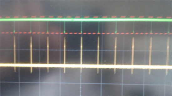
however,although my DRDY has signals out, I couldn't get the clk out . Also  i didn't get the reference voltage.

So  how could this happen?

Is there some help me ?

i have already read some post  here . But they all used the SPI interface of their MCU directly.i  tried to use  the STM32 spi interface to communicate with ADS1298.that is ok.

I just don't know what is wrong in my project ? that problem has puzzled me for morths.

Wish someone have done this already,very appreciate for your help.

  •  Hi,everyone.

    Now i used DSP to communicate with ADS1298.The mcbsp  supports SPI mode .i configed the MCBSP in SPI  master mode ,sending one element of 8bits .I want to enable the  internal clk output,the DC test signals,and just open the channel one.The below is my config:

      CS_reset;//here i used a GPIO to send the ads1298 cs signal,cs=0

      mcbsp_write(SDATAC_Command);
      delay(5);//wait 4 tclk
     
      for(i=0;i<3;i++)   //internal reference  43  00  C0
      {
           while(!MCBSP_xrdy(hMcbsp0));
          MCBSP_write(hMcbsp0,CONFIG3[i]);
         // delay(1);
      }
     for(i=0;i<3;i++)    //low power mode and internal oscillator output enable 41  00 26
     {
       while(!MCBSP_xrdy(hMcbsp0));
       MCBSP_write(hMcbsp0,CONFIG1[i]);// 41 00 26
      }
     for(i=0;i<10;i++)  //set 8 channels  address 05 80 80 80  80  80  80  80
     {
      while(!MCBSP_xrdy(hMcbsp0));
      MCBSP_write(hMcbsp0,ADS1298testcfg[i]);//45 07 05 80 80 80 80 80 80 80
     }
     for(i=0;i<3;i++)   //set internal test signals
     {
       while(!MCBSP_xrdy(hMcbsp0));
       MCBSP_write(hMcbsp0,CONFIG2[i]);// 42 00 13
     } 
      START_set; //  START  is pulled high
     mcbsp_write(RDATAC_Command);
     delay(5);

    Then i used mcbsp polling to receive data from the ads1298,  when i got the DRDY low signals.there would be 48bits data (24 status +24 data ) once a time.

    However i didin't get the clk signals at the oscilloscope on the clk pin.  and the  signals of   SPI_out  from the ads1298  were not  very clean.

    So i want to confirm the config above is right? and how to receive the data from the ADS1298 ?

    i will appreciate for your help.

  • Hi 秦,

    Can you post your schematic and timings please?  Reading the data from the ADS1298 has been discussed in quite a few posts here already.  Take a look at this one for a pretty comprehensive overview:

    http://e2e.ti.com/support/data_converters/precision_data_converters/f/73/p/105352/379169.aspx#379169


  • Hi qw,

    The problem here may be related to the way you apply chip select to the ADS1298 or perhaps a clock phase to data valid relationship.  Are you using FSx as chip select?  Can you post a screen shot of your timing?  Running a McBSP peripheral (which processor by the way?) should be no different than using a native 3-wire SPI peripheral.

  • 3qu for your reply,Tom

    Firstly,I used a GPIO pin  of my dsp board as the ads1298 chip select  TMS320C6713.Becasue I knew from the ads1298.pdf CS must remain low for the entire  command  when send multi-byte command .And I also put the CS low when i send a command. eg, cs low ,send SDATAC  command ,cs high ,cs low ,send config3 command(4300c0),cs high,cs  low .etc.also some delay is needed between them.

    Secondly,as my cpu clk is 50HZ which because i didn't use PLL to change the CPU clk, I used MCBSP register SRGR  to divide the clk ,just 1.25MHZ(sclk).

    lastly I send the command order directly as the ADS1298.pdf said.And in order to see my command order ,before i  download the code to test the ads1298,I gave a while(1)

    cycle out of my command code.and i debug it step by step,and then i run the code ,seeing in the scope ,the command order is correct.However when i connect the ads1298 board to the dsp ,I found just the DRDY coming out  250HZ,and the clk pin didn't come out,also the reference was wrong ,just 500mv more or less.

    As you first said to me ,i looked for the others'  post   here,but their problem couldn't sovle my problem  .so what  is the main point of my problem?

    Later i will get a screen shot of my timing to you .

    qw


  • Hi,everyone

    here are my photoes of the timing.

     -----------picture 1

     picture1: the green one is DRDY ,the yellow one is SCLK

    -------picture2

    picture2 is the smaller part of picture1,only one cycle

    ------picture3

    picture3:channel two(green ) is the SPI_OUT,channel one (yellow) is the sclk

    ------picture4

    as the same as picture 3

    -----picture5

    picture5:just one cycle of picture 4

    ------picture6

    picture6 :as same as picture 5,just one cycle of the SPI_out data .

    CS is  low  during the  data receiving. Then turn to high for a while.At last turn to low again.

    In my code ,i config the ADS1298 to output the internal clk(2.048MHZ).However when i run my project ,the clk pin is low all the time.

    Also the reference voltage is just 500mv more or less.

    Once i think my config register didn't download to the ADS1298. However  there is  DRDY signal.And the receive data(SPI_OUT pin) as picture 6 showed ,the first 8bits is  11000000, referred to the page 29  of the ads1298.pdf.I just don't know what is wrong ?what is the problem?

    wish your help,appreciate.


  • Hi qw,

    Can you possibly post your project file? I can't see the detail I am looking for. What is causing the voltage level changes?

    The code we wrote for the ADS1298ECGFE-PDK actually uses the McBSP from the TMS320VC5509, so this certainly is something that can be done as well on the TMS320C6713.

  • Hi ,Tom

    Tom Hendrick said:

    The code we wrote for the ADS1298ECGFE-PDK actually uses the McBSP from the TMS320VC5509, so this certainly is something that can be done as well on the TMS320C6713.


    In your reference code ,your group just use TMS320VC5509 SPI part to communicate with ads1298. Or maybe i miss the part you said above,could you send to me?

    In my project ,i just use the mcbsp of my dsp(TMS320C6713) to communicate with ADS1298.There is no spi port in my dsp mcu. 

    Below is my project .

    3036.mcbsp1.zip

    3QU  for your help

  • Hi,Tom

    what is going on?

    Do you find the problem?


  • Hi qw,

    No - not yet.  I've got your project to compile, but there is no output from the McBSP.  What hardware are you using? 

    The TMS320VC5509 uses the McBSP in 'clock stop' or SPI mode on our eval setup for the ADS1298.  The source code is located here:

    ftp://ftp.ti.com/pub/data_acquisition/ECG_FE/ADS1298/

    We keep /CS low and vary the frame length of the SDI/SDO depending on the command.  Have you determined what the delta drive level is in the serial interface?  Where is that coming from?  Are the over/undershoots from the lack of ground connections on the probes or are they real?


  • Hi,Tom

    my hardware include: TMS320C6713  board ,ADS1298-FE

    First ,you should connect them, include SPI port and some GPIO,and  5V ,GND .

    like:

    MCBSP_CLKX0---------------------SPI_CLK

    MCBSP_DX0-------------------------SPI_IN

    MCBSP_DR0------------------------SPI_OUT

    and  so no.

    The source code located at

    ftp://ftp.ti.com/pub/data_acquisition/ECG_FE/ADS1298/    need password to see.  

    Tom Hendrick said:

    Have you determined what the delta drive level is in the serial interface?  Where is that coming from?  Are the over/undershoots from the lack of ground connections on the probes or are they real?

    I am very sorry i didn't understand what do you mean  the delta drive level .

  • Hi qw,

    For the password, try ads1298.  For the 'delta drive level' I was referring to the screen shots you posted.  There are two distinct logic high levels, clearly seen in pictures 5 and 6.  You can also see the overshoot there as well.  I did get your code running this morning.

    The data read from/written to the ADS1298 should be considered valid on the falling SCLK edge.  I think if you expand your time base on the oscilloscope you will see that you are writing to the part with the data being valid on the rising clock edge.  I suggest you modify your MCBSP_CONFIG setup as follows:

    MCBSP_Config mcbspCfg0 = {
    MCBSP_SPCR_RMK(
    MCBSP_SPCR_FREE_DEFAULT,
    MCBSP_SPCR_SOFT_DEFAULT,
    MCBSP_SPCR_FRST_DEFAULT,
    MCBSP_SPCR_GRST_DEFAULT,
    MCBSP_SPCR_XINTM_DEFAULT,
    MCBSP_SPCR_XSYNCERR_DEFAULT,
    MCBSP_SPCR_XRST_DEFAULT,
    MCBSP_SPCR_DLB_DEFAULT,
    MCBSP_SPCR_RJUST_DEFAULT,
    MCBSP_SPCR_CLKSTP_NODELAY, /* CLKSTP=11b with CLKXP=0, clock starts with */
    MCBSP_SPCR_DXENA_OFF,             /* rising edge with NO delay */
    MCBSP_SPCR_RINTM_DEFAULT,
    MCBSP_SPCR_RSYNCERR_DEFAULT,
    MCBSP_SPCR_RRST_DEFAULT
    ), ...

  • thank you Tom.

    Now ,the internal clk is out and i can change the data rate. From this ,you may say ,i could control the ADS1298 now.

    however ,there are some other problems. Firstly ,the  scope of the internal clk is too low,just 800mv. The frequency is  correct,2.048MHZ.

    Secondly , the data of SPI_OUT pin, duiring the DRDY high period ,theoretically is low,here sometime is high and sometime is low.after a while ,the signal turn right,but just

    stay low for a while. Another ,I found that there was a  high pulse ahead the 48bits data .

    After init the ADS1298,then i should receive the data from the ADS1298.In my project i just use polling to config the ADS1298.Then i don't know how to receive from the ads1298,although i  know first should take a look at the DRDY signal .when the DRDY is low  ,the data is ready.I think here polling is not the best method .I have read the code you send to me,but i was puzzled bu the example. could you explain the main part of the example to me? especially the init ads1298 part and receive data from the ads1298 part.

    appreciate to Tom,  thank you very much for patiently help.

    qw.

  • qw,

    For the SDO under DRDY high, if you zoom in and around your data you should notice the the SDO will stay high if the last bit is a '1' and low if it is a '0', so that's to be expected.  For the leading SDO bit ahead of your SCLK, that should not be possible - the ADS1298 cannot clock out data by itself, it needs to see an SCLK.  Judging by the looks of the signals (the noise components visible in the clock and data), I believe you should focus on trying to clean up your transmission lines.  How are you connected into the C6713?  What are your power supply levels?  Not sure why you would only have an 800mv signal at the oscillator output - I would need to see your schematic and try to determine what might be causing that.

    On receiving data,  the conversion data comes out at the same time you transmit, just like it would be with the normal SPI interface - the code I pointed you has some components that are part of our file transfer setup for the ADS1298ECGFE-PDK.  The DSP 'guts' of the code are found in the t1298_fn.h, t1298_ob.c, the tidc_api.c and .h files and dc_conf.h.  The code actually interrupts on DRDY (not using poling) and reads data in blocks according to the block size set in the GUI for our hardware ((see ADS1298_readblock() in t1298_ob.c).

    Granted that code is a little harder to follow but what it boils down to is this - transmit data via McBSP, read back from the part and store the results, something like this for instance:

    myDRDY_ISR()

    {   

    /* Wait until a value is received then read it */
        while (!MCBSP_xrdy(hMcbsp0));
        MCBSP_write(hMcbsp0, RDATA );         
        ad_buffer[i++] = MCBSP_read(hMcbsp0);

    }

  • Hi,Tom

    3QU for your advice.

    Those days i did two things.First,check my own ads1298  board,welding and connection.Second, I made a  intensive study of the code you send to me .

    First, my ads1298  power 5V  is from  the DSP board  out . This 5V is from a switching (voltage) regulator,220V-----5v(1A). Should I change the power supply to a DC power supply device?The connection of ADS1298 and DSP6713board is like this:   DX0--------SPI_IN  ,   CLKX0-------SPI_CLK  ,   DR0-------SPI_OUT ,  GPIO_PIN9 ------SPI_CS  ,   GPIO_PIN11------CLKSEL  ,  GPIO_PIN12------PWDN ,  GPIO_PIN13------ RESET  ,  GPIO_PIN15-------SPI_START  ,  GPIO_PIN10------SPI_DRDY. I used some 30cms long   wires connect them.Are these wires too long ?

    Second,i had read t1298_ob.c ,t1298_fn.h , dc_conf.h very carefully.I got those informations.There have two interrupts--- ADS1298_rblock_finished and ADS1298_drdyISR.The first interrupt i knew to check whether the DMA transfer complete. The second interrupt is set in the function fo ADS1298_readblock().And  this function calls SubmitBlock().What does this use to be?What 's more ,ADS1298_control() function uses  to set all the ADS1298 regs.And also the ADS1298_configure() function uses  to call four init function,including InitDevice(),InitMcbsp(),InitRcvDma() and InitXmtDma().

    As you said ,

    Tom Hendrick said:
    the ADS1298 cannot clock out data by itself, it needs to see an SCLK.
    ,after config the ADS1298,when we use mcbsp to receive data from the ads1298,we should give enough sclk to the ads1298, especially in RDATAC mode. So how did you solve this in you project?And  what about DMA? What is the order of the functions above? What is the orde going on with the programm?

    Tom Hendrick said:

    myDRDY_ISR()

    {   

    /* Wait until a value is received then read it */
        while (!MCBSP_xrdy(hMcbsp0));
        MCBSP_write(hMcbsp0, RDATA );         
        ad_buffer[i++] = MCBSP_read(hMcbsp0);

    }

    About this RDATA mode,i want to say:if just one channel,there will be 48bites data ,how could you do this receving 48 bites  data?I know from the PDF MCBSP_read only can receive 32 bites data.So?Change the MCBSP configure?

    Another,ADS1298 transfer data when there is SCLK.So here ,you just send RDATA(8 bites),maybe subsequent data is 24 status bites and 2 channel data (48bites),so where is the SCLK?

    In my project I want to  do like this :first using polling to configure the ADS1298 ,then using DRDY interrupt to receving data from ADS1298,at last using EDMA to save or transfer data to do other operation.So how to arrange them?Especially how to receving data continuely in the DRDY interrupt  function?

    Very appreciate for your patient help.

  • Hi qw,

    Sorry for the delay - I was out of the office last week.  The signaling between the DSP and ADS1298 seems correct.  You mention that you have 30cm wires connecting the two boards, that's nearly 12 inches and I do think that is a little too long.  You are likely to pick up substantial amounts of noise. 

    I am glad you did a review of the code.  The working of the various functions essentially just sets up the McBSP port and collects data or sets the registers, there really is nothing else to it.  The code does modify the McBSP settings depending on what it is doing.  The port is changed between sending 8-bits of data to receiving 24-bits.  Forty-eight bits is just two transfers of 24, nothing else.


  • Hi ,Tom

    Now ,i changed the wires between ADS1298 and DSP to at most 15cm. And I checked my welding very carefully.

    So i downloaded the program. I got the  internal clk output. However,also just 1.2V.and i found other problems.Firstly,the reference voltage steady decline from 2.4V to 0v. I just didn't know how could this happen. Secondly,the ADS1298 IC is a  little hot.  For i just used  2K data rate and just only one channel,the data is not too large.Third,do you find that in my picture the spacing between the first data and the second data is longer than the others.However,i used the same code to read them.(just one channel here, so 48 bits data). 

    Other things,i want to know how to deal with the CS.i do like this. When giving the reseting signal, put the CS to low. Then send  the SDATAC command.put the cs high,waiting  10us ,then put the CS low,then send another register_CONFIG1,then put the cs high,waiting  10us ,then put the CS low...at last send RDATAC command ,then  CS_high----wait ---- CS_low,then use a while(1) to read data from ads1298.Is this right?

    IF i use 2.4V referrence , 2K data rate ,2.048 internal clk,1.25MHZ sclk, just one channel, 3V_AGND power supply,  internnal DC test signal, what is the data out of  SPI_OUT(ads1298).For the resolution is 24 bits,so the data is? And which parameter have an influence  on  the data'  precision?

    The code you give me,i know there are two interruputs__ DRDY and rblock_finished . As we should set the inerrupt,like '(void)IRQ_enable(DMA_getEventId(pADS->hDmaRcv))'. And i know where is the second interrupt setting.where is the first one  in the code? i am sorry i didn't found it .

    The last ,as you said the ADS1298 couldnot  send data without the sclk from the master, so how do you deal with the SCLK and read data? i mean the master must send some data to the slave ,so there will be the sclk,and the length as same as the data you send.so how do you do this?

    thanks

    qw    


  • Hi,Tom

    Are you here ?

    could you give me some advice about the problems i have talked above?

    very appreciate.

    thanks .

    qw